Recent technology advances have resulted in power being the major concern for digital design. In this chapter we address how transistor sizing affects the energy and delay of digital circuits. The state of the art in circuit design methodology (Logical Effort) is examined and we identify its limitations for design in the energy-delay space. We examine how to explore the entire energy-delay space for a circuit and present an approach for the design and analysis in the energydelay space which allows for energy reduction without performance penalty. Finally, we present techniques for the design of energy-efficient digital circuits.
Presents the President’s Message for this issue of the publication.
Carry tree sparseness is used in high-performance binary adders to achieve better energy-delay trade-off. To determine the energy optimal degree of sparseness, a detailed analysis is performed in this work. An analytical expression for the upper bound of sparseness is derived. The effect of increased sparseness on partial sum block and total energy is explored on 32-, 64-, 128-, and 256-bit adders. Higher degrees of sparseness in the carry generation block is achieved by employing parallel adders in the sum block instead of serial ripple carry adders. 64-bit adders with various sparseness degrees using leading addition algorithms are synthesized and optimized with a standard cell library in 45nm CMOS technology. Post layout simulations revealed that the optimal sparse carry tree adders provide up to 50% and 22% improvement in energy at same performance over full carry tree Kogge-Stone and Ladner-Fischer adder designs, respectively.
Presents the President's message for this issue of the publication.
This paper presents a soft error hardened latch suitable for reliable operation. The proposed circuit is aimed to tackle the particle hit effect on the internal nodes, external logic, as well as the pulse generator circuit. The hardening method is based on redundancy to protect internal nodes and filter out transients resulted from combinational logic. It also uses redundant clocking technique which results in more robustness. The circuit is designed in 90nm CMOS technology and simulated with the HSPICE. Simulation results indicate its lower-power and -delay, and ability to recover from single particle strike on internal and clock nodes, and input transient tolerance up to 120ps.
Provides a listing of the editorial board, current staff, committee members and society officers.
This paper presents a simple sizing method for low-power that is comparable in speed and simplicity to the Logical Effort sizing. Yet, the accuracy of the results is in the range of simulation errors. The method is two orders of magnitude faster than methods based on convex optimization, allowing to make quick design choices and architectural trade-offs. In the standard cell environment the method can reduce power by more than 30% over existing designs obtained using synthesis tools. These results are confirmed on examples implemented in 45nm process.
The concept of energy efficiency for data driven applications is proposed in this paper as a relationship between energy dissipation and throughput delay, on equal amounts of data processed, defined as energy per bit and bit rate. We investigated several degrees of parallelism in circuits with the same functionality in terms of delay and energy consumption. We modeled two scenarios in data driven systems and identified the optimal points for both, in our proposed design space.
Energy-efficient serial and parallel multiplier structures are explored to see their suitability in the low and ultra low power design regimes. 16×16-bit serial and state-of-art parallel multipliers are compared in 45nm CMOS. A multiplier structure is proposed by optimizing the architecture, gate sizes and the voltage supply. The proposed structure provides 15% more throughput as compared to two-cycle parallel multiplier with the same energy consumption for high speed applications. In the low speed design region, it provides 3.7X energy reduction compared to the serial multiplier.
EDITORIAL OFFICE PO Box 3014, Los Alamitos, CA 90720;(714) 821-8380; r. baldwin@ computer. org Unless otherwise stated, bylined articles, as well as product and service descriptions, reflect the author’s or firm’s opinion. Inclusion in IEEE Micro does not necessarily constitute endorsement by the IEEE or the IEEE Computer Society. All submissions are subject to editing for style, clarity, and length.
Exploration of energy & delay trade-offs requires a sizing solution for minimal energy under operating delay and output load constraints. In this work, a simple method called Constant Stage Effort Ratio (CSER) is proposed for minimal energy solution of digital circuits with a given target delay. The proposed method has a linear run-time dependence on the number of logic gates that is exponential for the optimal solution. As sample cases, the proposed algorithm is applied to parallel VLSI adders with varying bit-widths at 65nm CMOS technology. CSER sizing algorithm provides more than 300x run-time improvement compared to energy optimal solution with a worst case difference of 10% in energy for a 128-bits Kogge-Stone adder.
This paper introduces a novel Multi-mode Serial Link Controller (MMSLC) for logic physical layer (PHY) and data link layer (DLL) of USB 3.0, PCIe 2.0 and SATA 3.0. Functions defined in these protocols are grouped based on qualifying similarities and workload. The framework consists of a configurable circuit, programmable accelerator and event processor for flexible implementation. This MMSLC can essentially substitute for three individual link-controllers across protocols, thus achieving area reduction. An RTL level implementation is fulfilled and the synthesis results are shown at the end of this paper.
In this paper we present a new transistor sizing methodology called Free Power Recovery (FPR) for low power circuit design. The objective of this methodology is to minimize the total power of a circuit by accounting for node switching activities and leakage duty cycles (LDC). The methodology has been incorporated into the EinsTuner circuit tuning tool. EinsTuner automates the tuning process using state-of-the-art non-linear optimization solvers and fast circuit simulators. Node switching activities and LDC are integrated into the EinsTuner framework as parameter inputs to the FPR tuning mode. In FPR mode, the power is minimized using gate width reduction with respect to power properties of the node. The FPR methodology is evaluated on next generation microprocessor circuit designs. Power reduction results are compared with the results from the existing EinsTuner tuning methodology. The results show improvement in power reduction with the FPR optimization mode.
Unless otherwise stated, bylined articles, as well as product and service descriptions, reflect the author’s or firm’s opinion. Inclusion in IEEE Micro does not necessarily constitute endorsement by the IEEE or the IEEE Computer Society. All submissions are subject to editing for style, clarity, and length.
Booth encoding is believed to yield faster multiplier designs with higher energy consumption. 16×16-bit Booth and Non-Booth multipliers are analyzed in energy and delay space under varying constraints. It is shown that Non-Booth multipliers start to become more energy efficient for strict delay targets. In addition, novel 3:2 and 4:2 compressors are presented to save energy at the same target delay. The proposed compressors provide up to 20% energy reduction depending on the target delay at 65nm CMOS technology. Non-Booth multiplier implemented with the proposed compressors provides performance advantage as the voltage is scaled from its nominal value. Further, we examined all designs in 45nm, 32nm and 22nm CMOS technology nodes.
 Nikola Nedovic合作论文数University of California Davis27
 Bart R. Zeydel合作论文数22Aamir A. Farooqui合作论文数12
 Vladimir Stojanovic合作论文数Berkeley Wireless Research Center, University of California, Berkeley;Center for Energy Efficient Electronics Science, University of California, Berkeley;Berkeley Emerging Technologies Research Center, University of California, Berkeley12
 Dejan Markovic合作论文数Samueli School of Engineering, University of California, Los Angeles11
 Borivoje Nikolic合作论文数Department of Electrical Engineering and Computer Sciences, University of California at Berkeley;Berkeley Wireless Research Center, University of California at Berkeley10
 Mustafa Aktan合作论文数Boğaziçi University;Department of Electrical and Electronics Engineering;Department of Electrical and Electronics Engineering, Boğaziçi University10
 Ram Krishnamurthy合作论文数Circuit Research Lab, Intel Corporation9Hq Dao合作论文数8
 Dursun Baran合作论文数University of Texas at Dallas8Richard Mateosian合作论文数7Kevin W Rudd合作论文数7Richard H Stern合作论文数7Thomas Conte合作论文数7Xiaodong Zhang合作论文数7
 Mateo Valero合作论文数Department of Computer Architecture, Universitat Politecnica de Catalunya;Barcelona Supercomputing Center, Centro Nacional de Supercomputación7Marko Aleksic合作论文数Department of Electrical and Computer Engineering
University of California7David Villeger合作论文数Electrical and Computer Engineering Department;University of California Davis7
Mateo Valero合作论文数Department of Computer Architecture, Universitat Politecnica de Catalunya;Barcelona Supercomputing Center, Centro Nacional de Supercomputación7Marko Aleksic合作论文数Department of Electrical and Computer Engineering
University of California7David Villeger合作论文数Electrical and Computer Engineering Department;University of California Davis7 Ronny Ronen合作论文数Intel Corporation7
 Shane Greenstein合作论文数Harvard Business School, Harvard University7Marian Anderson合作论文数6Charles Moore合作论文数6Sandra Brown合作论文数6Michael Flynn合作论文数6Marc Tremblay合作论文数6Kemal Ebcioglu合作论文数6
 Pradeep Dubey合作论文数Parallel Computing Lab, Intel Corporation6
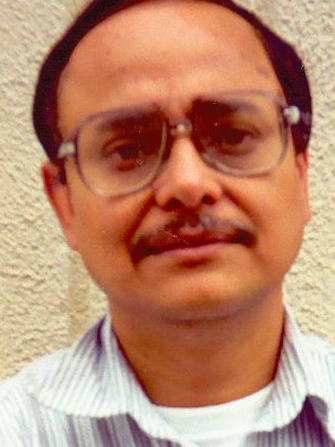 Pradip Bose合作论文数Department of Computer Science, IBM T.J. Watson Research Center6
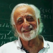 Yale N. Patt合作论文数High Performance Substrate/High Performance Systems Lab, Chandra Family Department of Electrical and Computer Engineering, Cockrell School of Engineering, The University of Texas at Austin6
 Lizy Kurian John合作论文数Department of Electrical and Computer Engineering, The University of Texas at Austin6Philip G. Emma合作论文数5Paul F. Stelling合作论文数5Thomas Centrella合作论文数5Robin Baldwin合作论文数5
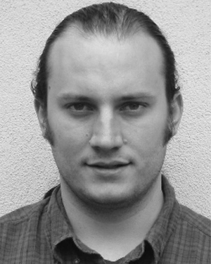 Christophe Giacomotto合作论文数5William W. Walker合作论文数U. S. Department of the Interior5
 Kevin Skadron合作论文数Department of Computer Science, School of Engineering and Applied Science, University of Virginia5Milena Vratonjic合作论文数5Evan Butterfield合作论文数4Cheryl Baltes合作论文数4Noel Deeley合作论文数4farzad chehrazi合作论文数4Tilman Wolf合作论文数4Joan Taylor合作论文数4
 Dragan Maksimovic合作论文数Department of Electrical, Computer & Energy Engineering, College of Engineering and Applied Science, University of Colorado Boulder4
 Sanu Mathew合作论文数Intel Corporation4K. Wayne Current合作论文数Department of Electrical and Computer Engineering :: University of California Davis4
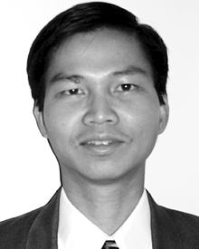 Hoang Q. Dao合作论文数4B Duchene合作论文数3




