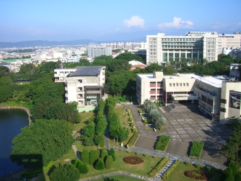
台湾交通大学(National Chiao Tung University,缩写为NCTU),简称台交,位于中国台湾新竹市,是台湾顶尖研究型重点大学之一,与台湾清华大学及新竹科学工业园区相邻,与中国大陆四所交大共同联合成立“交通大学校友总会”。 台湾交通大学为中等规模之研究性大学,以理工著称,在电子、资通讯及光电领域居于世界前列。 学校源头为1896年创立于上海的南洋公学、1896年创立于唐山的山海关北洋铁路官学堂。两岸分治后,上海原址改组为西安交通大学和上海交通大学。唐山、北京原址分别改组为西南交通大学和北京交通大学。1958年,交通大学继政治大学及清华大学之后在台复校,校址选定新竹市。 根据2016年5月学校官网显示,学校有光复校区、博爱校区、六家校区、台北校区、台南校区五个校区,校园占地面积88万平方米,校舍面积47.6024万平方米;开设18个学系,24个研究所;有教师715人,学生14141人。 2019年度,台湾交通大学位列2020QS世界大学排名第227位,2019世界大学学术排名501-600位。

Infrared unmanned aerial vehicle target detection is of great value in protecting national and personal security due to the inherent strong anti-interference capability of infrared sensors. Therefore, it has become an important area of research in remote sensing and computer vision. Influenced by long shooting distances and complex backgrounds, infrared unmanned aerial vehicle images often contain significant background noise and weak features, which pose significant challenges for infrared unmanned aerial vehicle target detection. In this work, we propose an attention-guided network for infrared unmanned aerial vehicle target detection. We first extract frames from videos in the Anti-unmanned aerial vehicle dataset and corrects incorrect labels, so that we can obtain the dataset used for model training. Then, we enhanced asymptotic feature pyramid network for the neck portion of the model, reducing the loss of small target features during network propagation. Next, we introduce efficient spatial coordinate attention to highlight the features of infrared unmanned aerial vehicle targets and enable the network to quickly focus on the regions of interest. Finally, to account for the varying aspect ratios of small targets, we employ the shape intersection over the union function as the bounding box loss function to improve the accuracy of target localization. The experimental results show that our network has achieved better performance than the state-of-the-art one-stage detection frameworks.
Object detection has advanced significantly, becoming essential in applications of internet of things (IoT) such as autonomous vehicle, mobile devices, smart home and intelligent transportation system. To overcome the performance limitations of single object detection models, these models are often combined with preprocessing techniques like multi-focus image fusion to enhance detection capabilities. Despite these enhancements, the robustness of such integrated systems against adversarial attacks remains a significant challenge, as prior research has primarily focused on individual detection models rather than the entire detection system. We propose UMOG (A universal adversarial example generation method for object detection system coupled with multi-focus image fusion model) method, a novel approach specifically designed to exploit vulnerabilities in object detection systems that incorporate multi-focus image fusion. UMOG hinges on two synergistic blocks: CAEGM crafts perturbations against detection outputs and iteratively audits them to keep single and fused models fooled, while NRM clamps the noise to Canny-dilated edges for minimal visibility. By exploiting the high-frequency-preserving trait of multi-focus fusion, the same perturbation slips through fusion and fools downstream detectors, exposing a neglected weak spot that transfers across fusion variants and detection backbones. Empirical tests show that such universal adversarial examples maintain high attack success rates against both standalone detectors and fusion-equipped pipelines, highlighting the urgent need for stronger defenses in real-world vision systems.
This paper presents a passive reconfigurable intermediate-frequency (IF) bandpass filter (BPF) based on GaAs technology, consisting of a reconfigurable high- and a low-pass filter (LPF) connected in cascade. It features low insertion loss (IL) and a high rejection level. To reduce the IL caused by reconfigurable elements, these components are mainly applied in the shunt branches rather than in the main signal paths, for the purpose of adjusting transmission zeros. An enhanced rejection level is achieved by incorporating fixed TZ attributed to the LPF section. To validate the proposed design, a circuit prototype is designed, fabricated, and tested using a 0.15-μm GaAs p-HEMT process It demonstrated a bandwidth tuning range of 0.4-1 GHz at a center frequency of 1.8 GHz, with an an in-band IL between 2.65 dB and 5.17 dB, a return loss better than 16 dB, an out-of-band(OOB) rejection of up to 37 dB, and far-band rejection exceeding 60 dB.
Ultra-wide-bandgap β-Ga2O3 films are advantageous for next-generation optoelectronic devices due to their wide bandgap and compatibility with scalable manufacturing processes. This study fabricated 20 nm polycrystalline β-Ga2O3 thin films on c-plane sapphire substrates via solution-based mist chemical vapor deposition (mist-CVD), a cost-effective, non-vacuum growth method. The structural, morphological, and optical characterization confirmed the successful formation of continuous β-Ga2O3 films. To examine carrier transport in ultrathin mist-CVD-grown β-Ga2O3, lateral metal–semiconductor-metal (MSM) devices with Ni/Au and Ti/Al/Ni/Au contacts were constructed utilizing channel spacings between 5 and 50 μm. The devices showed a turn-on voltage of 3.2 V and increased leakage currents in the 10–12 A range. The electrical measurements revealed poor rectification (0.9 at ± 10 V), suggesting that the transport is significantly influenced by non-ideal effects associated with the ultrathin polycrystalline film. This study indicates that grain-boundary defects, surface and interface states, contact-related constraints, and field-assisted conduction strongly influence the observed electrical behavior. While adequate rectification was not accomplished, this study serves as a proof of concept for ultrathin mist-CVD β-Ga2O3 films and provides a scalable, entirely non-vacuum method for incorporating β-Ga2O3 into lateral device architectures.
This work demonstrates interlayer-engineered top-gated vertical ferroelectric field-effect transistors (VFeFETs) featuring a stacked architecture with a 2-nm InOx vertical channel. A two-step low-temperature annealing scheme is employed to optimize ferroelectricity and device performance: an anneal at 400 °C for 30 s to crystallize the Hf0.5Zr0.5O2 (HZO) ferroelectric layer, followed by a treatment at 250 °C for 30 min that passivates defects in the InOx channel. Enabled by this annealing scheme, the SiO2-interlayer devices with channel length (Lch) of 82 nm exhibit tight and stable distributions of both high-threshold voltage (HVT) and low-threshold voltage (LVT). An average memory window (MW) of 1.38 V is achieved, with a maximum of 1.83 V. In contrast, the SiNx-interlayer devices show a broader distribution, which is attributed to stronger interfacial trapping. Nevertheless, by exploiting the interlayer-dependent VT shift, four distinguishable conductance states (2-bit/cell) are achieved, highlighting the potential of this architecture for high-density, low-power nonvolatile memory with a low thermal budget compatible with advanced 3D integration.





