Numerical modeling is used to study the characteristics of an ultra-wideband distributed probing system for different network configurations. An optimal configuration of the system is proposed. It is shown that range and transverse coordinate resolutions are determined by the characteristics of the probing pulse and can reach 2–3 centimeters, corresponding to an effective angular resolution of several tens of micro-radians.
A scheme is proposed for a specialized analog processor that uses a microwave photonics correlation receiver in the form of a matched filter to treat an ultra-wideband microwave signal. The operation of such a filter is investigated numerically, and its characteristics (potential performance and the accuracy of identifying the position of the maximum of the output signal) are determined.
Two ways of creating an optical comb in an optoelectronic oscillator are proposed and investigated. The first is based on using a multimode regime of operation in an optoelectronic oscillator; the second, on a modulation expansion of the laser line using high indices of modulation. Characteristics of the two schemes are investigated by means of numerical modeling.
We proposed and studied a new method which allows producing an optical frequency comb in an optoelectronic oscillator. In this method, comb parameters can be adjusted by controlling CW laser and microwave filter frequencies and amplitudes of modulating signals supplied to the arms of Mach-Zehnder modulator having two separate microwave inputs. Characteristics of the system were studied with numerical modeling for delay line and mictoresonator in the optoelectronic oscillator loop.
A method for generating an optical frequency comb in an optoelectronic oscillator is proposed and investigated. It is based on the modulation expansion of a laser line using large modulation indices. In the proposed scheme, a double-microwave-input amplitude modulator is used in a single-loop optoelectronic oscillator instead of a usual amplitude modulator, and an optical output is arranged after it. The circuit characteristics and parameters of the formed optical frequency comb and microwave oscillation are investigated using numerical simulation, which allows us to study highly nonlinear and multimode regimes. The advantage of the scheme is an easy control of all parameters of the optical frequency comb by changing the frequency of the CW laser, the average frequency of the microwave bandpass filter, and the amplitudes of the modulating signals applied to the modulator arms.
Formation of a reference frequency comb in a circuit comprising a highly stable continuous laser and an amplitude Mach- Zehnder modulator with two independent RF inputs working with large modulation index for use in a high-speed microwave photonics ADC with spectral-interval estimation is investigated by numerical simulation. In such ADCs, the entire spectrum of the input signal is divided by microwave photonics elements into spectral intervals, each of which uses a microwave photonics converter to transform the signal to an intermediate frequency (for each part of the spectrum of the microwave input signal, its own reference frequency is used for heterodyning). The requirements for a multimode source of optical reference frequencies for high-speed microwave photonics ADC are formulated. To study the characteristics of such a source, numerical modeling is carried out. It is shown that the frequency noise of the laser can be partially suppressed due to their compensation when converted to an intermediate frequency. Experimental study of the reference frequency comb generator layout showed a good agreement of the obtained characteristics with the results of numerical simulation.
Рассмотрены структурные схемы построения радиофотонного приемного канала. Предложена схема многоканального радиофотонного приемного тракта на основе лазеров с прямой модуляцией, увеличения количества каналов благодаря использованию дополнительного способа уплотнения на основе вортексов и преобразования входных высокочастотных сигналов на разностную частоту с использованием опорного электрооптического модулятора. Также предложен способ формирования радиофотонного АЦП в спектральной области с использованием комб-генератора на основе электрооптического модулятора Маха-Цандера в режиме перемодуляции. Для входных сигналов с ограниченной спектральной шириной может быть применен метод разделения сигнала на спектральные полосы с последующей обработкой в собственном канале, где ширина полосы подстраивается при помощи электронного АЦП, использующегося для оцифровки. В большинстве случаев выходной сигнал электронного АЦП позволяет получить необходимую информацию о входном сигнале без совместной обработки выходных сигналов со всех каналов; в противном случае к выходным сигналам со всех каналов может быть применено преобразование Фурье, и затем спектры выходных сигналов могут быть объединены для получения необходимого полного спектра широкополосного входного СВЧ сигнала. Для реализации данного метода может быть использован непрерывный лазер совместно с рядом электрооптических модуляторов, фильтров и других пассивных оптических компонентов. Использование амплитудных модуляторов совместно с фазовыми в сильно нелинейном режиме при достаточно высокой входной мощности СВЧ сигнала (перемодуляции) делает возможным создание комб-генератора с десятками равноудаленных в спектральной области частот с малой амплитудной неравномерностью, менее 1 дБ. Оценены эффективность метода радиофотонного АЦП с использованием спектральных интервалов. Получены оптимальные параметры системы. Показана возможность достижения 8–10 эффективных бит в цифровом сигнале для современных оптических элементов.
Comparative study of different architectures for microwave photonics frequency converters of microwave signals is presented. Characteristics of the receivers with different architectures are obtained with the help of numerical simulation. Experimental parameters for the prototypes of receivers show good agreement with the results of numerical simulation. It is shown that the signal-to-noise ratio can reach 60-70 for a carrier frequency of tens of gigahertz and a receiving bandwidth of several hundreds of megahertz
Implementation of photonic analog-to-digital convertor (ADC) using an optimal way of information parallelizing at the level of circuit solutions can significantly improve the performance of the total system (signal source - ADC - computing device). Traditional approach for fast photonic ADC uses processing every time-neighbor sample of input signal by its own channel. For the input signals with limited bandwidth, another approach can be used, in which every input signal spectral interval is processed by its own channel, and the width of the spectral interval is adjusted with the performance of an electronic ADC used for digitizing. In many cases, output signals of electronic ADCs are sufficient for obtaining necessary information from the input signal without joint processing of the output signals of all channels; otherwise, outputs of all channels can be Fourier-processed and concatenated to get complete spectrum of a wideband microwave input signal. For realization of this scheme, a mode locked stable laser together with an amplitude modulator and two combs of narrow band optical filters can be used. Alternatively, a mode locked laser can be replaced with a continuous wave (CW) laser together with a number of optical modulators. Performance capabilities for signal ADC using spectral intervals are estimated. Parameters for optimal system operation are derived. It is shown that, for modern optical elements, 8-10 effective bits can be achieved in the digitized signal.
Traditional architectures of fast electronic analog-to-digital conversion (ADC) are typically based on interleaving several lower sample rate digitizers, by combining which it is possible to realize high sample rate ADC. This approach requires high-precision timing and adds noises and harmonic distortions. Traditional architecture of fast photonic ADC is based on processing every time-neighbour sample of input signal by its own channel, however, this method typically requires high precision and expensive photonic components: femtosecond pulse source (mode-locked laser) with ultra-low timing jitter, optical fibers with high precision lengths, balanced photodetectors and others, which together form very unstable and bulky device. For the input signals with limited bandwidth, another approach for photonic ADC can be used, in which every input signal spectral interval is processed by its own channel, and the width of the spectral interval is adjusted with the performance of an electronic ADC used for digitizing. In many cases, joint processing of the output signals of all channels is not necessary; otherwise, outputs of all channels can be Fourier-processed and concatenated to get complete spectrum of a wideband microwave input signal. For realization of this scheme, two combs of narrow band optical filters can be used. Performance capabilities for signal ADC using spectral intervals are derived with numerical simulation and compared with experimental results. Parameters for optimal system operation are studied. It is shown that, for modern photonic components, 8-10 effective bits can be achieved in the digitized signal [1].
Main characteristics of a model of the microwave photonic receiving channel with optical heterodyning have been numerically simulated and experimentally investigated. The transducer is based on a twoarm (signal and reference) balanced circuit with a continuous wave laser, amplitude modulators, narrow-band optical filters, and a photodetector. The possibility of implementation of the receiving channel with a signal-to-noise ratio of up to 60–70 dB, a carrier frequency of up to 40 GHz and more, and a detection bandwidth of up to 1 GHz is demonstrated. It is shown that semiconductor lasers without outer stabilizing cavities can be used in an optical pumping source by means of compensation of the laser frequency noise. It has been found, that if the modulator working point corresponds to the optical carrier frequency suppression mode, the noise characteristics of the detector can be maintained without application of narrow-band optical filters.
Microwave photonic receiver for radar applications comprising a continuous wave laser together with amplitude modulators and narrow-band optical filters and converting radar signal to low (envelope) frequencies is considered. Possible characteristics of the receiver are estimated and different modes of its operation are discussed. It is shown that homodyne as well as heterodyne methods for transformation of the spectrum of the input microwave signal into the low frequency region can be used, and linearity of the transformation for these methods is studied. Also, the regime of the optical carrier suppression in modulators is considered. In this case, it is not necessary to use narrow-band optical filters in the scheme. It is shown that, for modern optical elements, signal-to-noise ratio at the output of the system can be 60-70 db and more for a microwave signal with a carrier frequency of tens of gigahertz and a frequency bandwidth of 100 MHz and more.
The possibility of formation of a virtual guiding system from a bunch of plasma channels of the filaments of femtosecond laser pulses for transmission of microwave radiation in air is considered. The effective conductivity and the skin depth of the laser plasma of such filaments are calculated for the microwave band. Optimum spatial configurations of plasma channels corresponding to a single-wire transmission line and a hollow cylindrical waveguide are proposed. Estimates of the energy loss of microwave radiation in plasma waveguides of various configurations are obtained.
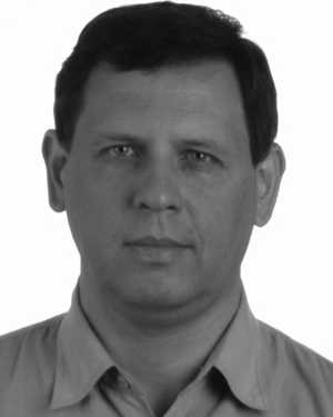 Victor V. Kulagin合作论文数19
 V. A. Cherepenin合作论文数11
 Sergey Kontorov合作论文数9V. N. Kornienko合作论文数9D. A. Prokhorov合作论文数8
 S. A. Shlenov合作论文数6
 A. E. Dormidonov合作论文数6Va Cherepenin合作论文数5
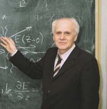 Valerii Kandidov合作论文数Faculty of Physics, Lomonosov Moscow State University5Denis Prokhorov合作论文数3Alexey N. Shulunov合作论文数2anatoly v rodin合作论文数1g s manukyan合作论文数1Vladimir N. Kornienko合作论文数1Nikolay I. Kargin合作论文数1V. D. Pismennyi合作论文数1Valery N. Kornienko合作论文数1V. A. Glukhikh合作论文数1Je Hee Lee合作论文数1
 Kyung-Han Hong合作论文数Massachusetts Institute of Technology1
 Olga Kosareva合作论文数P. N. Lebedev Physical Institute of the Russian Academy of Sciences;Faculty of Physics, Lomonosov Moscow State University1
 Yuri V. Gulyaev合作论文数Kotelnikov Institute of Radioengineering and Electronics, Russian Academy of Sciences1
 Hyyong Suk合作论文数Dept Phys & Photon Sci, Gwangju Inst Sci & Technol1Valerii P. Kandidov合作论文数1Yuri Gulyaev合作论文数1




