Human bodies damages induced by electronic equipment is into of physical and biological research since the revolutionary distribution in households of electric and electromagnetic devices e.g. radios, televisions, mobile phones, microwave ovens etc. This article is related to systematic examinations of magnetic fields generated by such a devices, e.g. televisions in their close vicinity and far away.
Protection of the environment is becoming more important role as pollution and magnetic loads from electronic devices are growing as never before. The radioactive background radiation does not explore explicit increase nevertheless more and more attention is paid to this. An increasing number of countries are paying more attention to measurements of the levels of background radiation from various radioactive sources and to the values of their exposure limits. It is known that the vast majority of background radiation in the enviroment comes from radioactive construction (buildings, roads, etc.) built by humans. It is important to understand its sources, evolution, determining parameters, etc. Radioactivity of the human-built environment is assessed on the basis of building materials, construction techniques, and dose-loading related to building technologies. The Department of General and Environmental Physics in the Juhasz Gyula Teacher Training College at the University of Szeged (Hungary) out radioactive measurements related to background radiation, especially the absorbed dose load from full gamma radiation. Among a wide range of measurements, the most important are: The power of radiation from walls and other parts of buildings. The field, such as radioactivity mapping of the environment. Using maps, we not only have actual data for the radioactivity, but we can follow the impact of the human-built environment (buildings, streets, etc.) on whole background radiation (Koteles, 1994).
Pulsed laser irradiated vanadium surface morphology under different ambient has been prepared and characterized using fractal dimension analysis method on scanning electron microscopy (SEM) images. In presence of different ambient, self-periodic and self-similar surface patterns (e.g. dots, islands, and pins) were grown and appeared in different shapes. The fractal dimension (FD) of this developed vanadium nanostructure was calculated by fractal box count method (FBM). The calculated fractal dimension (FD, Df) shows dependence on the different type on ambient and the number of laser shots.
In this work we present our results concerning to the nanostructure generation on vanadium surfaces by ultrashort pulsed laser irradiation. The melting free formation of these structures is very important in many fields of science and industry too. We obtain that the nanostructure forming process on vanadium surface is Stransky Krastanov type. The surface covering and the nano‐tower shape are depending on the ambient of the laser matter reaction.
Ultrafast changes in the crystal structure of GaAs induced by intense femtosecond laser pulses are detected and investigated. Atomic force microscopy and Raman microprobe analysis of the laser-treated area show centrosymmetric (disordered) features which are different from the original zinc-blend structure of the GaAs lattice. The frozen-in structure shows evidence for a special heat transfer from the laser-induced crater to the boundary, namely the heat has been transferred ballistically by a high-density electron-hole plasma.
Excimer laser pulses with wavelength of 308 nm, repetition rates of 1–10 Hz, pulse energies of 300–400 mJ, and pulse width of 20 ns are used to selectively seed palladium aggregates from a liquid-phase solution on polymer (polyimide) surfaces. The precursors used are PdCl2 in hydrochloric acid and Pd(CH3CO2)2 in acetic acid. The coverage of the polyimide with palladium aggregates is determined by the analysis of scanning electron microscopy measurements. Qualitative and quantitative analyses of seeded particles on polyimide (PI) are investigated by x-ray diffraction and transmission measurements. The amount of deposited palladium showed a quadratic dependence on the laser fluence reaching the surface. On the other hand, the coverage versus number of laser shots shows a square-root-like dependence. The palladium deposits also appear as amorphous and Pd[111] crystallites forms depending on the number of laser pulses. The roughness of a PI surface prior to seeding is modified mechanically and characterized by its fractal dimension. The fractal dimension of the samples varies between 2.3 and 2.7 for all the parameters applied, and the palladium deposition is found to be dependent on this dimension of the PI film.
In this work we give a phenomenological picture about the properties of the laser interaction with V2O5 single crystals. Our experiments show that the damaged region of the crystal surface is surrounded by a humped surface. The inner part of the examined region is covered by amorphous V2O5 and the outer part of this region has been raised by thermal shock of laser treatment. This heat effect produces the hump on the surface.
In this work, we present X-ray photoelectron spectroscopy (XPS) and X-ray diffraction (XRD) analysis of laser treated vanadium oxide sols. The films were also observed by transmission electron microscopy (TEM) and scanning electron microscopy (SEM) to reveal how the original xerogel structure changes into irregular shaped, layer structured V2O5 due to the laser radiation. XRD revealed that above 102W/cm2 the original xerogel structure disappears and above 129W/cm2 the films become totally polycrystalline with an orthorhombic structure. XPS spectra showed O/V ratio increment by using higher laser intensities.
Femtosecond (fs) laser pulse ablation (pulse duration of 150 fs, wavelength of 775 nm, repetition rate of 1 kHz) of single-crystalline TeO2 surfaces was performed in air using the direct focusing technique. The lateral and vertical dimensions of laser ablated craters as well as the laser damage thresholds were evaluated for different pulse numbers applied to the same spot. The joint observation using optical microscopy, atomic force microscopy and scanning electron microscopy revealed the surface morphology of the ablated craters and also showed that the ablation threshold depends significantly on the number of laser pulses applied to the same spot due to incubation effects. The incubation effects change the absorption processes involved in fs-laser ablation of the transparent material from multiphoton absorption to a single-photon absorption. These results are discussed on the basis of recent models of the interaction of fs-laser pulses with dielectrics.
Pulsed laser deposited nanocrystalline V2O5 thin films were characterized by X-ray diffraction (XRD), X-ray photoelectron spectroscopy (XPS), high-resolution transmission electron microscopy (HRTEM) and optical spectroscopy. The films were deposited on amorphous glass substrates, keeping the O-2 partial pressure at 13.33 Pa and the substrate temperature at 220 degrees C. The characteristics of the films were changed by varying the laser fluence and repetition rate. XRD revealed that films are nanocrystalline with an orthorhombic structure. XPS shows the sub-stoichiometry of the films, that generally relies on the fact that during the formation process of V2O5 films, lower valence oxides are also created. From the HRTEM images, we observed the size evolution and distribution characteristics of the clusters in the function of the laser fluence. From the spectral transmittance we determined the absorption edge using the Tauc plot. Calculation of the Bohr radius for V2O5 is also reported. (C) 2007 Elsevier B.V. All rights reserved.
In this paper a nonisothermal model which describes the oxide layer thickness evolution and the sample temperature variation in the case of a small vanadium plate in a cwCO(2) laser beam is considered. In the framework of the model the equilibrium temperature T*(P) of the sample; the equilibrium oxide layer thickness x*(P); the moment of time t(0)(P) when 1nm oxide layer thickness is achieved, the sample temperature T(t(0)(P)) at the moment t(0)(P)- the moment of time t(1)(P) when the equilibrium temperature is achieved; the oxide layer thickness x(t(1)(P)) at the moment then the equilibrium temperature is achieved;, the growth speed v(t(0)(P)) at the moment t(0)(P) and the growth speed v(t(1)(R)) at the moment t(1)(P) are computed in function of the laser power P, which varies in the range 4 - 25 [W]. It is shown that starting from the room temperature (T = 300[k]) if P increases, then T*(P) increases and x*(P) decreases at the beginning but after that increases t(0)(P) is of order 10(-9) [s] and it is constant; T(t(0)(P)) is practically equal to the starting room temperature;, t(1)(P) is of order 10(0)/10(1) [s] and decreases when P increases; x(t(1)(P)) is of order 10(-5) [m] and decreases when P increases; v(t(0)(P)) is of order 10(-1) [m/s] and it is constant; due to the evaporation v(t(1)(P)) is negative it is of order 10(-8) / 10(-9) [m/s] and decreases when P increases. In particular it is shown that the experimental results, presented in [7], concerning the oscillogram of the sample temperature, the evolution of the oxide layer thickness can be obtained with high accuracy in the framework of the model. It is found that the oxide layer thickness evolutions for P = 4 [W] and P = 17 [W] correspond to the two oxide types VO and V2O5, as is reported in [7]. How well the computed results are in agreement with other experimental results depends on the smallness of the effect of the processes which were not incorporated in the model. The advantage of this theoretical analysis is the possibility to obtain explicit results from which the limits of the model can be specified and special results can be gleaned. With this aim this study was undertaken.
The mathematical model describing $SiO_2$ layer growth presented in this paper is defined by the original Deal-Grove differential equation, used for describing oxide layer growth at constant temperature and by the heat balance equation, which describes the temperature evolution in the sample, when the injected power is constant. In this framework it is shown, that starting with a sample, which has an initial (natural) oxide layer thickness $x'$[m] and a temperature $T'=300$[K], and injecting in the growth system a constant power P[W], the oxide layer thickness x[m] evolves according to a law which is in a good agreement with results reported in the literature, both for thin and large oxide layer thicknesses. The computed evolution reveals that oxide layers of thickness below 10 nm grow in the transition period, i.e. during the period of time when the sample temperature $T$ increases from $T'$ and achieves the constant equilibrium temperature $T_0$ (which depends on the injected power $P$). Numerical examples are given for (100) and (111) oriented Si samples and the computed results are compared to the results reported in the literature.
Vanadium oxide thin films were prepared by sol–gel method, then subjected to Nd:YAG laser (CW, 1064nm) radiation. The characteristics of the films were changed by varying the intensity of the laser radiation. The nanocrystalline films were characterized by X-ray diffraction (XRD), X-ray photoelectron spectroscopy (XPS), transmission electron microscopy (TEM) and scanning electron microscopy (SEM). XRD revealed that above 102W/cm2 the original xerogel structure disappears and above 129W/cm2 the films become totally polycrystalline with an orthorhombic structure. From TEM observations, we can see that due to laser radiation, the originally fibrillar-like particles disappear and irregular shaped, layer structured V2O5 particles are created. From XPS spectra we can conclude that due to laser radiation the O/V ratio increased with higher intensities.
This study deals with the problem of ultrashort laser pulse damage of $TeO_2$ crystals. The laser wavelength dependent quantum energy lies in the almost transparent region of paratellurite, therefore the laser energy deposit occurs through nonlinear mechanism of multiphoton absorption of material. The time and position dependent optical breakdown is considered while the ($N_z$) in that case is smaller than unity.
The fractal dimension of finite quantum 1/f noise samples is determined in a simplified model with the Takens–Grassberger–Procaccia analysis of the time-series generated by this 1/f process.
In this work reactive pulsed laser deposition of molybdenum- and tungsten-nitride thin films is investigated. Metallic targets were ablated in low-pressure (1, 10 and 100 Pa) nitrogen atmosphere by KrF excimer laser pulses (fluence ∼6.5 J/cm2). Films were deposited on silicon wafers heated to ∼25, 250 and 500 °C. The characteristics of the films strongly depend on the N2 pressure. By increasing N2 pressure, the nitrogen content increases in the films, which leads to a monotonous increase of the electrical resistivity. Deposition rate decreases at 100 Pa as indicated by Rutherford backscattering spectrometry. At this pressure, hardness of the films significantly decreases also, as shown by microhardness measurements. X-ray diffractometry shows that films crystallinity is improved by increasing the substrate temperature. In addition, atomic force microscopy (AFM) and scanning electron microscopy (SEM) were applied for visualising the film surface.
Gold micropatterns are deposited from aqueous solutions of NaAuCl(4) on boron-doped Si(100) surfaces (rho = 1.5 x 10(-4) Omega m) using a focused Ar(+) laser beam (TEM(00), lambda = 488 nm, w(0) = 1.5 mum, P = 20-80 mW). The finite-element method employed for computing the surface temperature profiles reveals that the maximum temperature at the precursor/silicon interface increases only to the range 316-372 K, which is not high enough for chemical reactions with formaldehyde in the precursor. This suggests a different mechanism to be responsible for the reduction of gold ions, namely, changes in the surface potential of Si caused by the Dember and Seebeck effects.
Pulsed ArF laser annealing in air and in hydrogen atmosphere improves the optical properties of ZnO nanostructured films. Independently on the ambient atmosphere, laser annealing produces two major effects on the photoluminescence (PL) spectra: first, the efficiency of the exciton PL increases due to decrease of the number of non-radiative recombination centers; second, the intensity of the defect-related orange band decreases because of the removing of excessive oxygen trapped into the films during deposition. However, annealing in the ambient air also increases the intensity of the green band related to oxygen vacancies. We show that the combination of laser annealing and passivation of oxygen vacancies by hydrogen results in films free of defect-related emission and keeps intact their nanostructural character.
A localized step melting of lead foils under the influence of UV (λ = 308nm) laser pulses is investigated. Standard nanosecond pump-and-probe measurements are performed to follow the surface evolution of lead samples. The surface morphology of the irradiated parts of the samples is examined by conventional optical microscopy-densitometry and atomic force microscopy methods. The surface corrugation is characterized by profilometry (Dektak).
 I. Hevesi合作论文数34
 Robert Vajtai合作论文数Ken Kennedy Institute, Rice University;Department of Materials Science and NanoEngineering, Rice University27
 Thomas F. George合作论文数University of Missouri-St. Louis23K Bali合作论文数12Seppo Leppavuori合作论文数12
 Krisztian Kordas合作论文数Department of Electrical and Information Engineering, University of Oulu11E SZIL合作论文数8
 F V Bunkin合作论文数Academic Russia Academy of Sciences7
 Agneta M. Balint合作论文数Faculty of Physics;West University of Timisoara;Faculty of Physics, West University of Timisoara7Bs Lukyanchuk合作论文数6
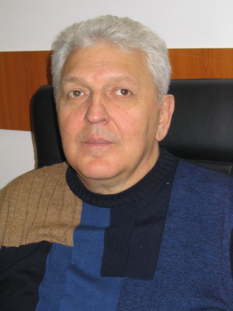 Ion Mihailescu合作论文数Faculty of Physics, University of Bucharest;Institute of Atomic Physics;Laser-Surface- Plasma Interactions Laboratory6
 Armando Luches合作论文数6Jozsef Bekesi合作论文数6Antti Uusimaki合作论文数6Janne Remes合作论文数5
 Boris Luk'yanchuk合作论文数Division of Physics and Applied Physics, School of Physical & Mathematical Sciences, Nanyang Technological University5Cs Beleznai合作论文数5Da Jelski合作论文数4Ferenc Ignacz合作论文数4
 Szabolcs Beke合作论文数Laser Technology Laboratory, RIKEN—Advanced Science Institute4N A Kirichenko合作论文数4Georgy a Shafeev合作论文数4GA Shafeev合作论文数3L. Kőrösi合作论文数3M. Füle合作论文数3w marine合作论文数3LB Kiss合作论文数3
 Elena Morozova合作论文数3S. Szatmári合作论文数3
 Robert Szabo合作论文数3Maria Aparecida Fernandez合作论文数3
 Paolo Mengucci合作论文数Dipartimento di Fisica e Ingegneria dei Materiali e del Territorio, Università Politecnica delle Marche3Giuseppe Majni合作论文数3G. Leggieri合作论文数3A. V. Simakhin合作论文数3И. Хевеши合作论文数3M.I. Török合作论文数3v a bobyrev合作论文数3
 Janos Kiss合作论文数Department of Orthopaedics, Semmelweis University3G. Taft合作论文数2Dt Alimov合作论文数2
 Aleksander V. Simakin合作论文数2J. Kovács合作论文数2
 M. Martino合作论文数Dip. Mat. e Fisica, Salento Univ.2
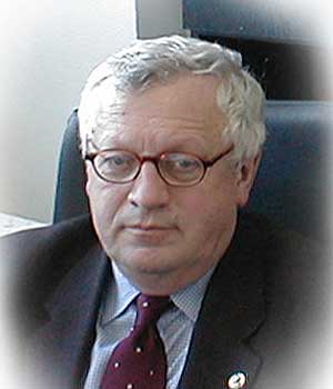 Vitaly I. Konov合作论文数Natural Scienses Center, A.M. Prokhorov General Physics Institute;Russian Academy of Sciences2
 Zsolt Toth合作论文数Research Group on Laser Physics, the Hungarian Academy of Sciences2Э. Сил合作论文数2Leona Nistor合作论文数2Peter Nagy合作论文数2




