This article discusses the main trends in the physics and preparation of metal oxides and summarizes the results of research published by SPQEO in this area over the past decade. The main metal oxides studied include ZnO, Zn1-xCdxO, Zn1-xCoxO, MgxZn1–xO, ZnO:Mn, VO2, ZrO2–Y2O3, TiO2, WO3, Gd2O3, Er2O3, WO3–CaO–SiO2–B2O3: Tb3+, Dy2O3, NiO, FexOy, Ga2O3, Al2O3, ITO, Ag2O and graphene oxide. These oxides were obtained by the following methods: sintering in air or in a stream of various gases, magnetron sputtering, atomic layer deposition, explosive evaporation, sol-gel, spin coating, spray pyrolysis, rapid thermal annealing, green synthesis from plant solutions, melt quenching, rapid thermal annealing, self-ignition, ion-plasma co-sputtering, vacuum sputtering, reactive ion beam sputtering, and the Hammer method. The electrical and optical properties of the studied oxides are illustrated.
The paper studies peculiarities of current transport in Au/Pt/Ni/diamond Schottky diodes with the hysteresis in current–voltage (I-V) characteristics and the nonlinear dependence of the barrier height φb on the applied voltage and proposes a method for determining basic parameters. Lateral diode structures were processed on boron-doped HPHT-diamond grown in the Fe-Al-B-C system and demonstrated barrier I-V characteristics with the exponential growth of the forward current of about eight orders of magnitude. It is shown that the voltage-dependent barrier height and hysteresis of the current-voltage characteristics can be explained by the presence of a thin dielectric gap at the metal-semiconductor interface and deep levels with lifetimes of the order of tens of seconds or more. Recharging of deep levels can significantly affect the parameters of the current-voltage characteristics. Three distinct regions were revealed. Excess current at zero voltage (region I) is related to deep-level recharge. Within regions II and III linear dependence of the φb on the applied voltage was observed. A linear dependence of the φb is related to the thermionic-field emission mechanism of current transport. Analysis of the temperature dependence I-V characteristics, capacitance-voltage (С-V) as well as frequency-capacitance (C-f) characteristics of arrays of HPHT diamond Schottky diodes yields information on the distribution of macro-defects, the state of the surface, and doping of the sub-surface region, which can be used for the improvement of the growth process and post-growth treatments for the development of diamond-based microelectronic devices.
The results of the Raman study of the apatite coatings, obtained by gas detonation deposition detonation spraying of the precursor salts on the titanium substrates are presented. The mixture of Ca(OH)(2) and (NH4)2HPO(4) salts at the molar ratio 5:3 was used as precursors. A detailed analysis of the most intense Raman band showed hydroxyapatite formation with a dominant contribution of the amorphous phase. The post-deposition thermal annealing at 640 degrees C for 30 min in the Ar atmosphere leads to the transformation of the amorphous hydroxylapatite into the crystalline one.
Relevance of recent research is important for scientists and journals reporting research results. There are many sources of prognoses and one of them is the Report of European Commission "Looking into the R&I future priorities 2025-2027". It predicts the importance of the following areas for users: healthcare, energy, climate, sustainability and digitalization. The Ukrainian journal Semiconductor Physics, Quantum Electronics and Optoelectronics (SPQEO) actually focuses on these areas and contributes to the development of related knowledge. Monitoring of last SPQEO issues shows some interesting results: (i) the effect of local field amplification, which causes emergence of ponder motive forces acting on viruses until destruction of viral envelopes; (ii) the methods of malignant tumors treatment taking into account their genesis mechanisms and focusing on correction of definite pathogenesis components, while being nontoxic for other organs and tissues; and (iii) manipulation of the spectral characteristics of a “polycarbonate matrix – gold nanostructures – HTTH dye” system due to influence of gold nanostructures. SPQEO paid attention to the improvement of solar cells (SCs) by considering physical effects such as the effect of space charge region (SCR) recombination on the key characteristics of high-efficiency silicon solar cells, such as photovoltaic conversion efficiency and open-circuit voltage, is not only dependent on the charge-carrier lifetime in the SCR, but also on the ratio of hole-to-electron-capture cross section, σp/σn. Non- traditional SCs were also considered: SCs with perovskite thin films, SCs comprising CdS/CIGS heterojunctions, and vitamin B12-patterned silicon hybrids based SCs. Moreover, SPQEO also covers research results in the fields of quantum devices, diamond- like and oxide films, and light-emitting diodes.
The Ukrainian journal Semiconductor Physics, Quantum Electronics and Optoelectronics (SPQEO) was launched in 1998 artificially combining three main areas of scientific activity inherent to the V. Lashkaryov Institute of Semiconductor Physics of the National Academy of Sciences of Ukraine, namely semiconductor physics, quantum electronics and optoelectronics. After a decade this artificial base turned into some kind of organic symbiosis, namely: (i) the main optoelectronic systems are based on semiconductor devices, for example, fiber-optic networks; (ii) semiconductor lasers dominate in a huge number of applications in quantum electronics; (iii) semiconductor physics proposes new types of LEDs with extremely high efficiency, and so on. This article is dedicated to the 25 th anniversary of SPQEO. According to the Google Scholar Citation statistics, above 1680 articles cited more than 7350 times in total were published in the journal from 1998 to 2023. The statistics of references of journal articles and the scientific areas of the most cited articles are presented.
The gas-detonation technique was used for the synthesis of biocompatible hydroxylapatite-based protective coatings on polymer and titanium substrates. Hydroxylapatite powder of high purity with a grain diameter of 50 µm was used as the raw material. The obtained coatings have the thickness close to 200 µm. It has been shown that the offered method enables to create of non-destructive hydroxylapatite-based coatings on polymer by varying the distance between the polymer target and the gun nozzle of gas- detonation setup. Using the data of Raman and X-ray measurements, it was ascertained that gas-detonation deposition doesn’t change the composition of the deposited material. The SEM investigation testifies that the formed hydroxylapatite-based coatings are porous. EPR studies have shown that there are no paramagnetic defects in the obtained coatings, and the coating itself has a higher radiation hardness as compared to the raw powder.
The active channels in AlGaN/GaN‐based heterostructures are studied under different applied electrical fields to identify the Joule heating factors affecting the temperature values in the channels. The temperature in active channels of two different lengths (30 and 180 µm) is characterized using optical methods, and electrical methods are used as a reference. The technique of optical thermometry is based on the data of micro‐photoluminescence and micro‐Raman experiments. The electrical method is based on the measurements of current–voltage characteristics for comparison. It is shown that photoluminescence‐ and electrical‐based temperature values demonstrate similar behavior and good correlation. The Raman‐based method, exploiting the temperature dependence of the frequency position of E 2 high vibrational band in GaN, shows a significant deviation compared with electrical‐ and luminescence‐based methods. This deviation is shown to be related to the residual mechanical strain in the layered structure and the formation of hot phonons. The influence of hot phonons and mechanical strain effects increases at high electrical load (>5 kV cm −1 ) and at high temperatures (>400 °C), respectively.
The theory of spin-orbit interaction, developed by E.I. Rashba more than 30 years ago, stimulated the rapid development of a new discipline – spintronics – the physics of processes and devices based on the control of spins. The paper summarizes achievements of Prof. Rashba in the early stage of his scientific researches, particularly those, which were performed in Ukraine. Among them, prediction of electric dipole spin resonance (EDSR), phase transitions in spin-orbit coupled systems driven by change of the Fermi surface topology, giant oscillator strength of impurity excitons, and coexistence of free and self-trapped excitons. Solid state physics is the basis of contemporary electronics and optoelectronics. Various electronic, optical, acoustical and other effects and processes in solid define performances of modern solid state devices. Multitude of groups and thousands researchers are involved in discovering, study and using relevant new phenomena. Among them, Professor Emmanuel Rashba with his outstanding results in physics of crystals is seen (rises) as a profound personality. His contribution in almost all branches of solid state physics cannot be exaggerated, some of his results have found important applications. Prof. E.I. Rashba is known as one of the leading theorists in Ukraine, in Soviet Union, and he continued the successful career in United States. Although many years have already passed, scientific community in Ukraine remembers Prof. E.I. Rashba and thankfully appreciates his impact to formation of condensed matter researches in our country. This short text is devoted to Prof. E.I. Rashba and is written on the occasion of his birthday.
We present calculations of frequency and wavevector dispersion of conductivity of two-dimensional electrons confined in AlGaN/GaN heterostructures at the arbitrary level of the degeneracy and the presence of strongly inelastic scattering mechanism by the optical phonons. We found that the high-frequency conductivity deviates from that of the standard Drude–Lorentz model and changes significantly at elevated temperature. The results were applied for simulation of the spectral characteristics of the grating-based plasmonic structure for wide temperature range. We found that thermal activation of the inelastic scattering leads to significant red-shift of the plasmon resonances. This facilitates refinement of interpretation of experimental results published in series of recent papers. We concluded that for AlGaN/GaN heterostructures, the electron effective mass changes in narrower diapason of 0.22me,…,0.26me, when temperature varies from 77 to 300 K. We suggest that found peculiarities of the high-frequency conductivity and its spatial dispersion are of a general character and can be important for high-frequency and high power devices based on AlGaN/GaN heterostructures.
Embedding nanocrystals (NCs) in polymer matrices is a way to protect NCs from degradation and tailor NC properties. The investigation of luminescent NCs in transparent polymers is important due to their perspective applications in photonics and bio-imaging, while NCs in conductive polymers can also be promising for photovoltaics, electroluminescence, and photodetectors. Here, we investigate the effects of different water-soluble polymers, such as polyvinyl alcohol (PVA), polyvinylpyrrolidone (PVP), polyethylene glycol (PEG), gelatine, and poly(3,4-ethylenedioxythiophene) polystyrene sulfonate (PEDOT:PSS), on the photoluminescence (PL) of colloidal ZnO NCs synthesized ex situ in dimethyl sulfoxide (DMSO) solvent. Based on the spectral and intensity changes in the NC PL spectra, caused by the polymer, we discuss possible recombination mechanisms of the NC PL and interactions between NCs and polymer. The major common effect of PVP, PEG, and PVA is the suppression of a defect-related PL band (DPL). The effect of the polymers is found to be more different from each other at low NC loading than at high loading. Gelatine causes an unexpectedly marked quenching of both excitonic (EPL) and DPL. The effect of PEDOT:PSS is relatively weak, as for conductive polymer, although distinct indications of structural and electronic changes in the polymer are found in Raman and X-ray photoemission spectra. For better understanding the redistribution of the photoexcited charge carrier over the NC states and electronic interaction with polymer, we performed experiments with a well-studied electron acceptor, MV2+.
Highly textured ZnO films are fabricated, the outer polar surface of which is decorated with copper complexes. The segregation of copper on the surface during growth is attributed to the manifestation of the Jahn–Teller effect.
A method of dynamic deformations has been proposed as a useful informative tool in the characterization of transportation properties of a two-dimensional electron gas (2DEG) in AlGaN/GaN heterostructures. It is found that the exposing of a sample to ultrasonic vibrations results in the persistent acousto-conductivity (PAC) which was observed up to room temperatures. The PAC behaves itself like persistent photoconductivity (PPC), and the carrier density in the 2DEG channel is primarily contributed by the transfer of electrons excited from traps (like DX centers) as a result of their reconstruction under the ultrasonic loading.
In this work, we have investigated the features of electron transport in AlGaN/GaN transistor-like heterostructures with nanowires of different width. These nanostructures are studied extensively because of their great electronic and sensing advantages for electronic biosensor applications. We study the depletion effects and impact of ultraviolet excitation on the electron transport in sets of nanowires of different width from 1110 down to 185 nm. We have found significant difference in electrical characteristic’s behavior between wide (1110…480 nm) and narrow (280…185 nm) nanowires and have observed regions related to space-charge-limited transport for the narrowest nanowires. Also, we obtained evident dependence of nanowire’s current-voltage characteristics on the wavelength and energy of UV excitation. External UV excitation allows us to control the depletion widths in nanowires and effectively tune space-charge-limited transport.
January 15 marked the 100th anniversary of a famous Ukrainian scientist in the field of optics and spectroscopy, a talented mentor of young scientists, twice winner of the State Prize of Ukraine in Science and Technology (1981, 1986), Honored Worker of Science and Technology of Ukraine (1991), laureate of the V.I. Vernadsky Golden Medal of the NAS of Ukraine (2010), Doctor of Physical and Mathematical Sciences (1961), Professor, Academician of the NAS of Ukraine (1982) Mykhailo P. Lysytsia.
The temperature dependences of the specific contact resistance of silicon ρc with a doping step are measured experimentally and described theoretically. The measurements are performed in the temperature range from 4.2 to 380 K. It is established that the contacts of the studied Au–Ti–Pd–n+–n-Si structures are ohmic. It is shown that minimal ρc is implemented at T = 75 K. Its value rises both with a decrease in temperature (due to the freezing effect) and with an increase in temperature (due to the electron-enriched layer at the boundary with the bulk material). It is established that the bulk electron concentration strongly decreases in the near-contact region in a layer with a thickness on the order of one micron due to the compensation of silicon by deep acceptors appearing because of the formation of a rather high vacancy concentration during stress relaxation and the appearance of a high dislocation density, as well as due to their diffusion from the contact after heating to 450°C. The data on the occurrence of vacancy-type defects are confirmed by X-ray measurements. The dislocation density in the studied structures is also estimated from X-ray measurements.
The method of processing the data of electrophysical investigations of ohmic contacts has been developed. It allows obtaining more accurate results of measuring the contact resistance and additional information by analyzing the statistical and spatial distribution of input data. To test the method, the Au-Ge-TiB2-Au contact to n-n(+)-GaAs was used. The analysis of frequency distribution for the total resistance, specific contact resistance and surface resistance of semiconductor has been carried out. The spatial distribution of these parameters has been analyzed. With taking the linear gradient of specific resistivity into account, the value of the contact resistance has been clarified. We have achieved reduction of half-width of the distribution by 14%, that is, reduction of the error in determining the contact resistance. The method has been developed for correct analyzing the impacts of technological treatments and degradation processes and has been oriented on research purposes. Evaluation of the gradient distributions of the contact resistance and the resistance of semiconductor can be used to identify the defects in the technological processes of manufacturing devices.
Nitridation of silicon surface is an important step in GaN or AlN nanostructures growth process which determines quality of fabricated devices. In this work modeling of gas-surface reaction of the Si(111) surface nitridation was performed using density functional theory calculations. We show that interface structure corresponding to first stoichiometric Si3N4 monolayer may be generated in a great number of different ways by means of vacancy-assisted mechanism. The nearly continuum distribution of total energies may be associated with such structures formed after exothermic reaction with considerable energy gain. Nevertheless founded global minimum corresponds to abrupt interface and crystalline-like Si3N4 monolayer structure. Suggested mechanism of silicon nitride film growth is based on the calculated energy barriers for diffusion of volatile species such as N, N-2, SiN and SiN2 which are building blocks for the growth of Si3N4 film. At first stage atomic nitrogen diffusion from vacuum to substrate occurs. Then silicon vacancies in substrate and volatile SiN radicals are formed. The back diffusion of SiN from substrate to Si3N4-vacuum side is the main mechanism responsible for silicon nitride film growth.
The effects of built-in deformation and stress relaxation on the structural and optical properties for a 21-period AlN/GaN superlattice (SL) after implantation with argon ions have been studied. Upon implantation, the satellites’ peaks in the X-ray diffraction spectra shift toward the smaller angles which indicate decreasing of tensile deformation in SL by the value of Δc/c = 0.28%. The SIMS analysis showed that the sputtering rate for the initial sample decreases with depth, which is explained by the effect of varying deformation fields in SL and a faster etching of SL layers with a larger deformation magnitude. The change in the sputtering rate of individual layers of SL after implantation also correlates well with the magnitude of deformation. Implantation of Ar+ ions into SL leads to relaxation of the system and more homogeneous distribution of bond energy in individual layers of superlattice. The Raman spectra of the implanted SL are characterized with a low-frequency shoulder in the most intense band of the GaN layer E2 (high), which testifies partial stress relaxation in SL. Thus, based on a comprehensive study of the initial and implanted SL, it has been concluded that point defects that occur during implantation activate the process of dislocations nucleation in the superlattice/GaN buffer layer interface, which reduces the compressive stresses in the GaN layers of SL.
Biomorphic carbon matrices (BCMs) were produced by pyrolysis from wood species of different forest and garden trees, after which the as-prepared BCMs were converted to SiC ceramics through their impregnation with liquid silicon and further heat-treatment. Both types of obtained samples were studied by scanning electron microscopy (SEM), Raman scattering (RS), and electron spin resonance (ESR) methods. The SEM data reveal that all BCM samples contain large (10–50 μm) and small (1–5 μm) micro-pores with surface densities ∼109 m−2 and 1011 m−2, respectively. Analysis of RS allowed to estimate carbon cluster sizes of about 5–11 nm depending on the sample type. The study of the electronic structure using ESR spectroscopy is carried out for BCM and SiC ceramics samples. Using theoretical analysis of the ESR spectra, it was found that spin resonance in BCMs is due to the contribution of three spin systems: free electron spins, “pseudo-free” electron spins from the tail of density states below the conduction band, and localized spins at dangling carbon bonds (DCBs). Their contributions depend on the ratio of different structural phases such as sp2-hybridized graphite-like carbon network and amorphous carbon phase. For most BCM samples, the large ESR line width is dramatically narrowed when samples are pumped out due to the exclusion of the broadening effect of molecular oxygen. The transformation of BCM into SiC by impregnation with liquid silicon can be clearly traced in the Raman spectra and in the ESR spectra. It is established that the electronic properties of synthesized SiC ceramics are due to the presence of residual graphite-like carbon nanoclusters.
We experimentally demonstrate that the conductivity of graded AlxGa1-xN increases as a function of the magnitude of the Al concentration gradient (%Al/nm) due to polarization doping effects, without the use of impurity dopants. Using three up/down-graded AlxGa1-xN nanolayers with Al gradients ranging from ∼0.16 to ∼0.28%Al/nm combined in one structure, the effects of polarization engineering for localized electric fields and current transport were investigated. Cross-sectional Kelvin probe force microscopy and conductive atomic force microscopy were used to directly probe the electrical properties of the films with spatial resolution along the thickness of the growth. The experimental profiles of the built-in electric fields and the spreading current found in the graded layers are shown to be consistent with simulations of the field distribution as well as of the electron and hole densities. Finally, it was directly observed that for gradients less than 0.28%Al/nm the native n-type donors still limit polarization-induced hole doping, making p-type conductivity still a challenge due to background impurities and defects.
 Raisa Konakova合作论文数101
 N. S. Boltovets合作论文数55
 Svetlana Vitusevich合作论文数50
 Norbert Klein合作论文数Department of Materials, Faculty of Engineering, Imperial College London45Viktor V Milenin合作论文数43
 S. V. Danylyuk合作论文数42SA Vitusevich合作论文数38
 Vasyl Peter Kladko合作论文数Lashkaryov Institute of Semiconductor Physics, National Academy of Sciences of Ukraine38
 Yaroslav Ya. Kudryk合作论文数35
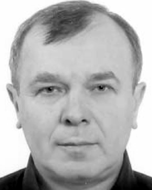 M. V. Petrychuk合作论文数34Vladimir N Ivanov合作论文数30
 Andrian V. Kuchuk合作论文数Lashkaryov Institute of Semiconductor Physics, National Academy of Sciences of Ukraine30
 Volodymyr Sheremet合作论文数28A. V. Sachenko合作论文数26
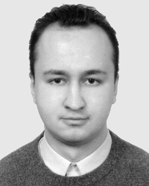 Andrey M. Kurakin合作论文数26
 Viacheslav a Kochelap合作论文数Lashkaryov Institute of Semiconductor Physics18S. M. Komirenko合作论文数15OP GORODNICHII合作论文数15
 Andrii Naumov合作论文数14L. M. Kapitanchuk合作论文数14
 B. A. Danilchenko合作论文数14NV SHEVCHENKO合作论文数13
 Volodymyr O. Yukhymchuk合作论文数Institute of Semiconductor Physics13Yu. N. Sveshnikov合作论文数12
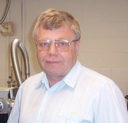 Victor Strelchuk合作论文数National Academy of Sciences of Ukraine Institute of Semiconductor Physics12
 Hryhorii Stanchu合作论文数V. Lashkaryov Institute of Semiconductor Physics, National Academy of Sciences of Ukraine11
 Mykhailo Valakh合作论文数11A. Mąkosa合作论文数11A. Yu. Avksentyev合作论文数11A. Vertiatchikh合作论文数10G. J. Salamo合作论文数10Lf Eastman合作论文数10Hans Lüth合作论文数Halbleiter-Nanoelektronik (PGI-9), Peter Grunberg Institut, Forschungszentrum Julich10
 Hilde Hardtdegen合作论文数Institut für Schicht- und Ionentechnik (ISI),, Forschungszentrum Jülich10
 P M Lytvyn合作论文数V. E. Lashkarev Institute of Semiconductor Physics, National Academy of Sciences of Ukraine10
 Oksana Lytvyn合作论文数Institute of Semiconductor Physics pr. Nauki 45, National Academy of Sciences of Ukraine10Yu. I. Mazur合作论文数10m e ware合作论文数9LN KRAVCHENKO合作论文数9PI BARANSKII合作论文数9
 Mohamed Henini合作论文数School of Physics and Astronomy, Faculty of Science, University of Nottingham;Nottingham Nanotechnology and Nanoscience Centre, University of Nottingham9
 Viktor Sydoruk合作论文数9
 Vinayak Tilak合作论文数9
 Alexander V Bobyl合作论文数9Joseph A. Smart合作论文数IS , Inc9
 Yuriy I. Mazur合作论文数Institute for Nanoscience and Engineering, University of Arkansas9
 V. S. Kiselov合作论文数8V. P. Klad’ko合作论文数8T. Figielski合作论文数Institute of Physics;Polish Academy of Sciences;Institute of Physics, Polish Academy of Sciences8




