We investigate a three-dimensional simulation method for finite-sized photonic-crystal surface-emitting lasers (PCSELs) based on guided mode expansion (GME), which is capable of estimating lateral and vertical modal loss rates. The approach generalizes established three-dimensional coupled-wave theory (3D-CWT) by considering an arbitrarily large set of basis functions including higher-order lateral and vertical (waveguide) modes. Detailed comparisons between the two methods for an UV-C AlGaN PCSEL with hexagonal lattice reveal corrections with respect to modal wavelengths and threshold gains. Furthermore, we demonstrate that interactions with higher-order waveguide modes, which can only be taken into account by GME, could enable the experimentally observed wide-angle lasing modes that distort the far-field.
Semiconductor membranes are widely used in research fields that target medical, biological, environmental, and optical applications. Often such membranes derive their functionality from a nanopatterning, which challenges the determination of their optical, electronic, mechanical, and thermal properties. In this work, we demonstrate the noninvasive, all-optical thermal characterization of approximately-800-nm-thick and approximately-150-& micro;m-wide membranes that consist mainly of wurtzite GaN and a stack of In0.15Ga0.85N quantum wells as a built-in light source. Because of their application in photonics, e.g., for vertical-cavity surface-emitting lasers, such photonic membranes are bright light emitters, which challenges their thermal characterization by optical means. We combine top-view two-laser Raman thermometry (2LRT) with time-resolved photoluminescence spectroscopy to extract the in-plane thermal conductivity kappa in plane of these membranes, which represents a notable difference from previous studies on epitaxial GaN films. Thus, we can disentangle the entire laser-induced power balance. Thermal imaging by Raman spectroscopy yields kappa in plane = 165+16-14 W m-1 K-1 for the best membrane. This result compares well with kappa in plane = 177 W m-1 K-1 obtained by ab initio simulations based on a solution of the linearized phonon Boltzmann transport equation, including three-and four-phonon scattering, as well as phonon-isotope and phonon-boundary scattering. Furthermore, we study how kappa in plane is affected by a roughening of the membrane's back side and additional semiconductor layers. For the membrane with the roughest back side, we observe a reduction of kappa in plane by almost 40%, which is accompanied by an anisotropy of kappa in plane due to etch channel formation. Thanks to the 2LRT approach, such variations and anisotropies of kappa in plane become accessible to the experimentalist via highly spatially resolved temperature maps.
We demonstrate bottom-emitting GaAs vertical-cavity surface-emitting lasers (VCSELs) incorporating a buried subwavelength grating in the top, highly reflective distributed Bragg reflector (DBR), with oxide aperture diameters ranging from 2 to 6. The buried grating successfully pins the polarization for aperture diameters up to 4 μm, and the 3 μm aperture VCSELs achieve single-mode, single-polarization operation, delivering 3.9 mW of output power with a side-mode suppression ratio exceeding 30 dB and an orthogonal polarization suppression ratio (OPSR) of 20 dB. Simulations and measurements indicate that the buried surface-etched grating can only weakly influence the lasing mode in the bottom-emitting configuration, thereby preventing polarization pinning of higher-order modes in larger-aperture VCSELs. The surface-etched gratings introduce minor degradation in threshold current, slope efficiency, and beam profile.
Semiconductor membranes are widely used in research fields that target medical, biological, environmental, and optical applications. Often such membranes derive their functionality from a nanopatterning, which challenges the determination of their optical, electronic, mechanical, and thermal properties. In this work, we demonstrate the noninvasive, all-optical thermal characterization of approximately-800-nm-thick and approximately-150- μ m -wide membranes that consist mainly of wurtzite Ga N and a stack of In 0.15 Ga 0.85 N quantum wells as a built-in light source. Because of their application in photonics, e.g., for vertical-cavity surface-emitting lasers, such photonic membranes are bright light emitters, which challenges their thermal characterization by optical means. We combine top-view two-laser Raman thermometry (2LRT) with time-resolved photoluminescence spectroscopy to extract the in-plane thermal conductivity κ in~plane of these membranes, which represents a notable difference from previous studies on epitaxial Ga N films. Thus, we can disentangle the entire laser-induced power balance. Thermal imaging by Raman spectroscopy yields κ in plane = 165 − 14 + 16 W m − 1 K − 1 for the best membrane. This result compares well with κ in plane = 177 W m − 1 K − 1 obtained by simulations based on a solution of the linearized phonon Boltzmann transport equation, including three- and four-phonon scattering, as well as phonon-isotope and phonon-boundary scattering. Furthermore, we study how κ in plane is affected by a roughening of the membrane’s back side and additional semiconductor layers. For the membrane with the roughest back side, we observe a reduction of κ in plane by almost 40%, which is accompanied by an anisotropy of κ in plane due to etch channel formation. Thanks to the 2LRT approach, such variations and anisotropies of κ in plane become accessible to the experimentalist via highly spatially resolved temperature maps.
In vertical‐cavity surface‐emitting lasers (VCSELs), the cavity length defines the resonance wavelength, which is directly related to the laser detuning, that is, the difference between resonance wavelength and gain peak. A low detuning maximizes the modal gain leading to a reduction of the threshold. Therefore, controlling the cavity length of VCSELs is of great importance. Here optically pumped ultraviolet‐C (wavelength 280 nm) VCSELs with precise cavity length control are demonstrated. The VCSEL structure is formed by an AlN cavity with 5 Al 0.40 Ga 0.60 /Al 0.70 Ga 0.30 N quantum wells and a top HfO 2 spacer layer with dielectric SiO 2 /HfO 2 distributed Bragg reflectors on both sides of the cavity. To access the N‐face side of the cavity, a new methodology referred to as photo‐assisted electrochemical etching is employed for substrate removal. Across a 0.9 mm 1.2 mm area, the lasing wavelength varies a maximum of 1.17 nm between different UVC VCSELs, exhibiting threshold pump power densities from 0.7 MW/cm 2 to 3.7 MW/cm 2 and detuning values between 0 to 2 nm. The results show that VCSELs with a cavity length variation lower than 1 can be obtained with this technology.
Abstract 2D transition metal dichalcogenide (TMD) materials have attracted interest due to their remarkable excitonic, optical, electrical, and mechanical properties, which are dependent on their crystal structure. Consequently, controlling the crystal structure of these materials is essential for fine-tuning their performance, e.g., linear and nonlinear optical, as well as charge transport properties. While various phase-switching TMD materials are available, their transitions are often irreversible. Here, we investigate the mechanism of a light-induced reversible phase transition in mono- and bilayer rhenium disulfide (ReS2). Our observations, based on transmission electron microscopy, nonlinear spectroscopy, and density functional theory, reveal a transition from the ground $${\rm{T}}^{\prime\prime}$$ T ″ (double-distorted T) to the metastable $${\rm{H}}^{\prime}$$ H ′ (distorted H) phase under femtosecond laser irradiation or influence of highly-energetic electrons. We show that the formation of sulfur vacancies facilitates this phenomenon. Our findings pave the way toward manipulating the crystal structure of ReS2 and possibly its heterostructures.
Different mirror concepts are being explored in parallel for III-N vertical-cavity surface-emitting lasers (VCSELs), each with their own pros and cons. A general belief is that epitaxial distributed Bragg reflectors (DBRs) offer a VCSEL with superior thermal performance compared to all-dielectric DBRs. We here show that this is not the case for GaN-based VCSELs designed for 440 nm emission with cavity lengths ≥10λ due to a laterally dominated heat flow caused by the high thermal conductivity of GaN cavity material in contrast to the lower thermally conductive DBRs. If the same cavity design that is used for blue GaN VCSELs is applied to ultraviolet-C (UVC) AlGaN-VCSELs this will lead to detrimentally high internal temperatures (up to 370°C) due to the very low thermal conductivity of AlGaN which would prevent lasing. Increasing the cavity length to 30λ reduces the thermal resistance from 4400 K/W to 2600 K/W, but this is not enough. To drastically lower the internal temperature, we propose adding 300 nm AlN spacer layers to the AlGaN cavity, which reduces thermal resistance to 1100 K/W, which is similar to that of blue VCSELs. The low thermal resistance of this design shows promise for realizing electrically injected, continuous-wave AlGaN-based UVC VCSELs.
We study transverse mode control in InGaN-based blue vertical-cavity surface-emitting lasers (VCSELs) by investigating the most common index-guiding structure which is an etched nano-cylinder with and without a refill of $\text{SiO}_{2}$. Using $2-8 \mu ~\mathrm{m}$ wide aperture diameters, we evaluate key performance metrics-threshold material gain $(g_{\text{t h}})$ and modal discrimination. The etched aperture with a 5 nm etch depth exhibited the lowest threshold material gain among the designs studied. Notably, this configuration showed the smallest increase in threshold material gain when the aperture diameter was reduced from $8 \mu ~\mathrm{m}$ to $2 \mu ~\mathrm{m}$. Furthermore, when decreasing the aperture from $8 \mu ~\mathrm{m}$ to $\text{4} \mu \mathrm{m}$, the $g_{\text{th }}$ for the fundamental $\text{L P}_{01}$ mode increased by just $95 ~\text{cm}^{-1}$, while still achieving a high modal discrimination of $395 ~\text{cm}^{-1}$. These results highlight the ability of the etched aperture to maintain low loss and strong mode selectivity over a practical range of aperture sizes.
In vertical-cavity surface-emitting lasers (VCSELs), the lasing wavelength is defined by the longitudinal cavity mode. The spectral misalignment between the resonance wavelength and the gain peak, known as detuning, is crucial for the device performance. Temperature also influences detuning since the gain peak red shifts faster than the resonance wavelength when the temperature increases. These important effects have not been explored in detail for ultraviolet (UV) VCSELs despite the significant heating that is expected due to high electrical resistance and high thermal impedance. Here, we studied the threshold and detuning dependence in optically pumped AlGaN-based UVB and UVC VCSELs with different cavity lengths operated at different temperatures. The cavity lengths of the VCSELs, fabricated from the same epitaxial material, are varied by post-growth deposition of HfO2 spacer layers with different thicknesses. The results show a strong relation between the threshold and the detuning, where VCSELs have thresholds around 5 MW/cm2 for a nominal (operational) detuning of −2.5 nm (∼−1 nm), and below 1 MW/cm2 when the nominal (operational) detuning is set between 2 and 3 nm (1–3 nm) with a minimum threshold of 0.23 MW/cm2. Additionally, the temperature dependence of the VCSELs' thresholds is investigated and compared by temperature-dependent photoluminescence and an empirical relation. The VCSELs with lower thresholds at room temperature are, on average, 20 times less sensitive to temperature than those with higher thresholds at room temperature, suggesting that VCSELs with a nominal detuning of 2–3 nm are the optimum design choice.
Today's ultraviolet lasers are bulky, expensive, have low power-conversion efficiency, and usually suffer from poor beam quality. Semiconductor lasers have addressed these issues in the visible and infrared parts of the electromagnetic spectrum; but in the ultraviolet, they are just starting to see the light of day. Edge-emitting semiconductor lasers are the only ones demonstrated under electrical injection in the deep-ultraviolet (<280 nm) and they inherently suffer from poor beam qualities, multiple modes, and catastrophic optical damage to the mirror. The first deep-UV photonic crystal surface-emitting lasers are demonstrated here. The devices show single-mode emission around 279 nm with less than1(degrees)beam divergence. They require a specific design to overcome optical scattering and the low refractive index that otherwise prohibits a 2D standing optical field. The optically pumped deep-ultraviolet photonic crystal surface-emitting lasers offer drastically improved beam quality and provide an important step toward low-divergent, watt-class, electrically-driven UV PCSELs.
We present a comparative study of vertical and lateral loss estimation in photonic-crystal surface-emitting lasers (PCSELs), focusing on how finite-size effects depend on the choice of infinite-structure band model. To analyze these effects, we introduce a k-space weighted loss estimation (kSWLE) framework that can be applied to any infinite-structure band model, and we contrast its predictions with those of finite coupled-wave theory (finite-CWT), which inherently relies on the infinite-CWT bandstructure. The kSWLE approach provides a semi-analytical means of estimating radiative and lateral losses by integrating band-dependent quantities over a Gaussian k-space envelope determined by the device size. We apply kSWLE using both CWT and guided-mode expansion (GME) bandstructure models, enabling a direct comparison of how different infinite-structure descriptions influence the predicted losses and spectral properties. In regimes where the lasing mode is dominated by a single band and has a spectrally compact k-space distribution, kSWLE reproduces similar scaling trends as finite-CWT. However, for small devices or at specific fill factors, the mode has a broader k-space distribution with contributions from multiple bands, leading to ambiguous mode classification and increased deviation between models. These results highlight the strengths and limitations of each modelling strategy and establish kSWLE as a practical tool for evaluating finite-size effects in PCSELs.
We demonstrate the first electrically injected AlGaN-based ultraviolet-B resonant-cavity light-emitting diode (RCLED). The devices feature dielectric SiO2/HfO2 distributed Bragg reflectors enabled by tunnel junctions (TJs) for lateral current spreading. A highly doped n++-AlGaN/n++-GaN/p++-AlGaN TJ and a top n-AlGaN current spreading layer are used as transparent contacts, resulting in a good current spreading up to an active region mesa diameter of 120 μm. To access the N-face side of the device, the substrate is removed by electrochemically etching a sacrificial n-AlGaN layer, leading to a smooth underetched surface without evident parasitic etching in the n- and n++-doped layers of the device. The RCLEDs show a narrow emission spectrum with a full width at half-maximum (FWHM) of 4.3 nm compared to 9.4 nm for an ordinary LED and a more directional emission pattern with an angular FWHM of 52° for the resonance at 310 nm in comparison to ∼126° for an LED. Additionally, the RCLEDs show a much more stable emission spectrum with temperature with a red-shift of the electroluminescence peak of about ∼18 pm/K and a negligible change of the FWHM compared to LEDs, which shift ∼30 pm/K and show spectrum broadening with temperature. The demonstration of those devices, where a highly reflective mirror is spatially separated from an ohmic metal contact, opens up a new design space to potentially increase the poor light extraction efficiency in UV LEDs and is an important step toward electrically injected UV vertical-cavity surface-emitting lasers.
Compared to the maturity of today's blue laser diodes, which exhibit high efficiencies, low threshold currents, and long lifetimes, deep-ultraviolet (<280 nm) lasers have essentially just been born. We have only recently witnessed the first deep-UV, continuous-wave edge-emitting lasers operating at room temperature under electrical injection. And more complex laser structures in the deep-UV, such as vertical-cavity surface-emitting lasers and photonic crystal surface emitting lasers, are even further behind, having only been demonstrated under pulsed optical pumping. Among the many difficulties in transitioning from blue to deep-UV are the problems of efficient electrical injection, creation of optical waveguides and cavities in materials with low refractive index contrast, and high material defect densities. The question is, are these problems fundamental limitations to the technology, or just temporary growing pains to be overcome with hard work and persistence as we push lasers deeper into unseen wavelengths and frontiers?
The 2022 edition of the 9th International Workshop on Nitride Semiconductors (IWN) took place in Berlin, Germany, from October 9 to 14, 2022. The conference was chaired by Michael Kneissl (TU Berlin) and Jürgen Christen (University of Magdeburg). This important biennial event encompasses all aspects of III-nitride semiconductor science, engineering, and industry. The 2022 workshop continued the tradition of successful gatherings in various locations: Kanazawa, Japan (2818), Orlando, USA (2016), Wrocław, Poland (2014), Sapporo, Japan (2012), Tampa, USA (2010), Montreux, Switzerland (2008), Kyoto, Japan (2006), Pittsburgh, USA (2004), Aachen, Germany (2002), and Nagoya, Japan (2000). The participation at IWN 2022 in Berlin surpassed expectations following a two-year break due to the pandemic, with over 800 scientists representing 32 countries in attendance. The topics of the workshop ranged from novel nitride materials and nanostructures, to growth and fabrication, to characterization and fundamental physics, to electrical and optical devices. Two tutorial speakers (Andreas Waag, TU Braunschweig) and Chris Van de Walle (UCSB) opened the workshop, by discussing GaN-based micro-LEDs and point defects, respectively. Excellent presentations were given by six plenary speakers, who covered a wide range of topics of great interest to the community: Hiroshi Amano (Nagoya University) discussed about deep UV laser diodes, as an example of overcoming the semiconducting limits; Stacia Keller (UCSB) talked about lattice constant engineering for long wavelength nitride emitters; Matteo Meneghini (University of Padova) gave a presentation on defect- and reliability-related aspects, covering both GaN electronics and optoelectronics; Herbert Pairitsch (Infineon) gave a perspective on the applicability of recent advances in material research performed within the research project UltimateGaN; Euijoon Yoon (Seoul National University) gave an overview of recent progress and prospects of micro-LEDs grown on sapphire nano-membranes; Huili Grace Xing (Cornell University) gave a talk entitled “Reveal the true self of GaN by tunneling and avalanche”. The program was then enriched by the presentations of 67 invited speakers, 251 oral presenters, and 416 poster presentations, who covered all topics of interest for optoelectronic and electronic applications of GaN. The workshop organizers express their gratitude to the plenary and invited speakers, rump session chairs, panelists, and short-course presenters for their exceptional contributions to an engaging workshop. They would also like to recognize the industrial sponsors for their generous financial support. Additionally, the program committee's relentless efforts in soliciting and reviewing abstracts are greatly appreciated. A total of 62 submissions were received for the conference publications in the special issues of physica status solidi (a) and (b). All submissions underwent the standard peer-review process of the journals. Out of these submissions, 39 were selected for publication in physica status solidi (a), and 16 were chosen for publication in physica status solidi (b), all featured in a dedicated issue of pss. Among these, two were Review papers: an article entitled “Recent Progress of E-mode GaN MIS-HEMTs with Hybrid Ferroelectric Charge Trap Gate (FEG-HEMT) for Power Switching Applications”, by Jui-Sheng Wu, Edward Yi Chang et al. (National Yang Ming Chiao Tung University) [Phys. Status Solidi A 2023, 220, 2300018], and a paper entitled “On the Origin of the Yellow Luminescence Band in GaN”, by Michael A. Reshchikov (Virginia Commonwealth University) [Phys. Status Solidi B 2023, 260, 2200488]. The published articles encompass a comprehensive array of topics that were addressed during the workshop. Our appreciation goes to Gaia Tomasello and Stefan Hildebrandt for their valuable editorial peer-review work and to Heike Höpcke and Matt Lock for the post-acceptance assembly of this publication. In conclusion, we extend our gratitude to all the workshop attendees who actively contributed to making IWN 2022 a lively and enjoyable event. We eagerly anticipate the opportunity to reunite with you in O'ahu (Hawaii) for the next International Workshop on Nitride Semiconductors in November 2024. Michael Kneissl, TU Berlin (Germany) Jürgen Christen, University of Magdeburg (Germany) Conference Chairs Axel Hoffmann, TU Berlin (Germany) Bo Monemar, Linköping University (Sweden) Honorary Chairs Tim Wernicke, TU Berlin (Germany) Conference Secretary Ulrich Schwarz, TU Chemnitz (Germany) Local Chair Åsa Haglund, Chalmers University of Technology (Sweden) Matteo Meneghini, University of Padova (Italy) Guest Editors and Publication Chairs
We daily rely upon vertical-cavity surface-emitting lasers (VCSELs) for facial recognition and data communication. These lasers are now experiencing exponential growth and serves in other applications as well such as oxygen monitoring in combustion processes and in anesthetized patients in hospitals and as a source of heating in industry in the form of a large-sized array. The large interest for this laser class is linked to its beneficial qualities such as low threshold current, circular-symmetric low-divergent output beam, high efficiency, compactness, and low fabrication cost due to on-wafer testing. Due to these advantages, there is a strong push to realize VCSELs in other wavelength regimes, beyond the commercially available infrared and red. This would open completely new markets such as flood lights, projectors, sterilization, and medical diagnosis and treatment.
Ultraviolet light-emitting diodes (LEDs) suffer from a low wall-plug efficiency, which is to a large extent limited by the poor light extraction efficiency (LEE). A thin-film flip-chip (TFFC) design with a roughened N-polar AlGaN surface can substantially improve this. We here demonstrate an enabling technology to realize TFFC LEDs emitting in the UVB range (280-320 nm), which includes standard LED processing in combination with electrochemical etching to remove the substrate. The integration of the electro-chemical etching is achieved by epitaxial sacrificial and etch block layers in combination with encapsulation of the LED. The LEE was enhanced by around 25% when the N-polar AlGaN side of the TFFC LEDs was chemically roughened, reaching an external quantum efficiency of 2.25%. By further optimizing the surface structure, our ray-tracing simulations predict a higher LEE from the TFFC LEDs than flip-chip LEDs and a resulting higher wall-plug efficiency.
A concept for vertical‐cavity surface‐emitting lasers (VCSELs) is proposed and demonstrated to obtain a lasing wavelength with unprecedented temperature stability. The concept is based on incorporating a dielectric material with a negative thermo‐optic coefficient, d n /d T , in the distributed Bragg reflectors (DBRs) to compensate the positive d n /d T of the semiconductor cavity. In a short cavity, the optical field has a significant overlap with the DBRs, and the redshift of the lasing wavelength caused by the semiconductor cavity can be compensated by the negative d n /d T of the DBRs. Here, proof of this concept is presented for optically‐pumped VCSELs emitting at 310 nm, demonstrating a lasing wavelength that even blueshifts by less than 0.1 nm over an 80 °C range with a maximum slope of –3.4 pm K −1 . This is to be compared with a redshift of 1–1.5 nm over the same temperature range reported for III‐nitride blue‐emitting VCSELs. Furthermore, this method can also be implemented in VCSELs with longer cavity lengths by including a dielectric layer between the semiconductor and the DBR. The approach used here to obtain a temperature‐stable lasing wavelength is generic and can therefore be applied to VCSELs in all material systems and lasing wavelengths.
In recent years, there has been tremendous improvement in the performance of blue-emitting vertical-cavity surface-emitting lasers (VCSELs) and they are now on the cusp of commercialization. We will summarize state-of-the-art results and outline the main challenges in extending the emission wavelength into the ultraviolet (UV). Our method to simultaneously achieve high-reflectivity mirrors and good cavity length control by selective electrochemical etching has been essential to demonstrate the world’s first UV-B VCSEL. The use of dielectric mirrors, where one material has a negative thermo-optical coefficient, counteracts the inherent red-shift of the resonance wavelength, enabling a temperature-stable emission.
We will give an overview of state-of-the-art results and challenges to achieve high-performing III-nitride vertical-cavity surface-emitting lasers (VCSELs), with a particular focus on the requirements to push the emission wavelength into the ultraviolet (UV). Our method to simultaneously achieve high-reflectivity mirrors and good cavity length control by electrochemical etching enabled the world’s first UV-B VCSEL. The use of dielectric mirrors yielded lasers with a very temperature-stable emission wavelength thanks to the negative thermo-optic coefficient of the mirrors. We have used the same etch methodology to also lift-off fully processed LEDs from their growth substrate to improve the light extraction efficiency.
 Johan Gustavsson合作论文数Photonics Laboratory, Chalmers University of Technology113
 Anders Larsson合作论文数NVIDIA86
 Petter Westbergh合作论文数Photon Lab, Chalmers53
 Jörgen Bengtsson合作论文数Photonics Laboratory, Department of Microtechnology and Nanoscience, Chalmers University of Technology31benjamin kogel合作论文数25
 Filip Hjort合作论文数Department of Microtechnology and Nanoscience, Chalmers University of Technology24
 Hashemi Ehsan合作论文数20Tim Wernicke合作论文数18
 Joachim Ciers合作论文数Tech Univ Chemnitz, Chair Measurement & Sensor Technol, D-09126 Chemnitz, Germany18
 Michael Kneissl合作论文数Institute of Solid State Physics, Faculty II – Mathematics and Natural Sciences, Technische Universität Berlin;Ferdinand-Braun-Institut, Leibniz-Institut für Höchstfrequenztechnik18
 Peter Modh合作论文数Photonics Laboratory, Chalmers University of Technology16
 Haglund, E.P.合作论文数Dept. of Microtechnol. & Nanosci. (MC2), Chalmers Univ. of Technol.;c;Dept. of Microtechnol. & Nanosci. (MC2), Chalmers Univ. of Technol.14
 Michael Bergmann合作论文数13Martin Stattin合作论文数12Johannes Enslin合作论文数Inst Solid State Phys, Tech Univ Berlin11Tim Kolbe合作论文数11
 Krzysztof Szczerba合作论文数Clinic of Internal and Occupational Diseases;Medical Academy;Clinic of Internal and Occupational Diseases, Medical Academy10
 Emanuel P. Haglund合作论文数9Rashid Safaisini合作论文数9
 Nicolas Grandjean合作论文数Laboratory of Advanced Semiconductors for Photonics and Electronics, Institute of Physics, School of Basic Sciences, Ecole Polytechnique Federale de Lausanne8
 Pierluigi Debernardi合作论文数Istituto di Elettronica e di Ingegneria dell'Informazione e delle Telecomunicazioni, Consiglio Nazionale delle Ricerche, Politecnico di Torino8
 Munise Cobet合作论文数7Christina Carlsson合作论文数6
 Peter Andrekson合作论文数Department of Microtechnology and Nanoscience, Chalmers University of Technology6
 Tien-Chang Lu (盧廷昌)合作论文数Department of Photonics, National Yang Ming Chiao Tung University;Tin Ka Ping Opto-Electronics Research Center, National Yang Ming Chiao Tung University;Advanced Nanophotonics Lab, National Yang Ming Chiao Tung University6Tsu-Chi Chang合作论文数5
 Lars Magnus Ingemar Karlsson合作论文数Department of Microtechnology and Nanoscience, Chalmers University of Technology5
 Markus Christian Amann合作论文数Walter Schottky Institut, Technische Universität München5
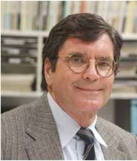 Dieter H. Bimberg合作论文数Bimberg Chinese-German Center for Green Photonics, Changchun Institute of Optics, Fine Mechanics and Physics, Chinese Academy of Sciences5
 Tommy Ive合作论文数University of California Materials Department5Gatien Cosendey合作论文数Inst Condensed Matter Phys, Ecole Polytech Fed Lausanne5
 Josip Vukusic合作论文数Department of Microtechnology and Nanoscience;Chalmers University of Technology;Department of Microtechnology and Nanoscience, Chalmers University of Technology5
 Piotr Jedrasik合作论文数5Giulia Cardinali合作论文数4J-F Carlin合作论文数4
 Mattias Karl Gustavsson合作论文数4
 Martin Guttmann合作论文数Inst Solid State Phys, Tech Univ Berlin4
 Lars Persson合作论文数Research Institute of Industrial Economics;School of Economics and Management, Lund University;IIES, Department of Economics, Stockholm University;Centre for Economic Policy Research;Ifo Institute4
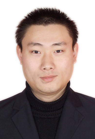 Jie Sun (孙杰)合作论文数School of Chemical Engineering and Technology, Xi'an Jiaotong University4Andrew Joel合作论文数4
 David Adolph合作论文数4
 Christian Grasse合作论文数4
 Wayne V. Sorin合作论文数Hewlett Packard Labs, Hewlett Packard Enterprise4
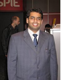 Prashant P. Baveja合作论文数4
 David Fattal合作论文数Leia Inc.4michael tan合作论文数3Nando Prokop合作论文数3




