A new process combining inductive plasma and electromagnetic stirring of molten silicon in a cold crucible has been developed to refine upgraded metallurgical silicon. The addition of reactive gases to the plasma makes it possible to volatilize impurities at the liquid silicon surface. The process has been studied both from a thermodynamic and a kinetic point of view. The concentration of boron impurities decreased from 15 ppmw in the raw material to less than 2 ppmw after plasma treatment. The most volatile form of boron was BOH, which was obtained by treatment with a mixture of oxygen and hydrogen. The volatilization rate depends on the oxygen and hydrogen flow rates. The limitation in boron volatilization is due to the formation, at high oxygen flow rate, of a silica layer at the surface of the molten silicon, which results in a dramatic drop of the volatilization rate. In contrast to boron, the concentration of phosphorus was reduced by only a factor of two, although the remainder seems to be electrically neutral. Thermodynamic study suggests that phosphorus could be trapped as phosphate in combination with metallic impurities or as aluminium phosphide. Cells made of material produced using this technique exhibited a conversion efficiency of 12.4 %.
Local thermodynamic equilibrium (LTE), frequently used as first approximation in modeling of thermal plasma processes, is sometimes unable to explain experimental results. It is particularly true near a wall and a surface impacted by the plasma jet. In this work, a 2-D custom model using the CFD commercial code Fluent was developed for argon-oxygen inductively coupled plasma (ICP) at atmospheric pressure. The assumption of thermal equilibrium was made but not that of chemical equilibrium. The transport properties were calculated using higher-order approximation of Chapman-Enskog theory. Reaction kinetics rates of dissociation and ionization were also considered. The model was applied to a process torch used for carving experiments on graphite, and the distribution of reactive species brought to the surface was analyzed in terms of reaction rate distribution: the experimental effect of different injection geometries on the distribution of the reaction rate is qualitatively reproduced by the model.
This article gives an up-date on the progress of the French PHOTOSIL project from a technical and an economical point of view. During the last 5 years, the French PHOTOSIL consortium formed by FerroPEM, CEAINES, CNRS SiMAP and APOLLON SOLAR has been working on a combination of new, innovative up-grading and purification techniques for MG Silicon on an industrial pilot level, to arrive at UMG Silicon that is compatible with the purity and economical requirements of the PV industry. The objectives of this project are production costs 15% solar cell efficiencies on multi-crystalline wafers from ingots made of 100% UMG Silicon and a material yield of >85% after crystallisation.
n-Type silicon wafers present some definite advantages for the photovoltaic industry, mainly due to the low capture cross sections of minority carriers for most metallic impurities. This peculiarity is beneficial for multicrystalline silicon (mc-Si) wafers in which the interaction between crystallographic defects and impurities is the main source of recombination centres. Most importantly, this peculiarity could be of a great interest when mc-Si ingots are produced directly from upgraded and purified metallurgical silicon feedstock. It is of a paramount importance to verify if the advantages of conventional n-type silicon also characterizes n-type wafers provided by a direct metallurgical route. It is found, in raw wafers., that minority carrier diffusion lengths are three times higher in n-type than in p-type wafers, when the wafers art cut from the same ingot, where the bottom is p-type and the top is n-type, due to the difference in the segregation coefficients of doping elements (boron and phosphorus). After different processing steps and gettering treatments the minority carrier diffusion lengths are always neatly larger in it-type than in p-type wafers The results confirm the interest for n-type silicon. Copyright (C) 2009 John Wiley & Sons, Ltd.
The effect of the reactant gas injection mode into inductively coupled plasma has been investigated, through the volatilization reaction of a graphite target submitted to argon-oxygen plasma. A graphite disk is positioned at different distances under the plasma torch. The addition of oxygen to the plasma results in a carving, of the graphite surface, which depend on the injection mode: into the outer, the intermediate or the inner argon flow. The mass losses permit to evaluate the global efficiency. The profile of the graphite surface at the end of the operation reflects the distribution of the reactive species. The graphite is heated by induction in order to stabilise its temperature between 1500 and 1800 K and to obtain stable reaction conditions. The most efficient, from the point of view of the reactive gas, consists in addition to the inner flow. The most homogeneous volatilization is obtained when the reactant is added to the outer flow.
Gettering treatments such as phosphorus diffusion and aluminium–silicon alloying have been applied to multicrystalline silicon wafers prepared from upgraded metallurgical feedstock. Purification of the feedstock results of plasma torch treatment and directional solidification. Minority carrier diffusion lengths Ln are close to 40μm in the raw wafers and increase up to 150μm after phosphorus plus Al–Si getterings. Improvements are limited by the presence of residual metallic impurities, mainly slow diffusers like aluminium, and also by the high doping level.
N-type silicon wafers present some definite advantages for photovoltaics, mainly due to the low capture cross sections of minority carriers for most metallic impurities. This peculiarity is beneficial for multicrystalline silicon (mc-Si) wafers. Most importantly, this peculiarity could be of a great interest when mc-Si ingots are produced directly from upgraded and purified metallurgical silicon feedstock. It is of a paramount importance to verify if the advantages of conventional n-type silicon also characterises n-type wafers provided by the direct metallurgical route. It is found, in raw wafers, that minority carrier diffusion lengths are 3 times higher in n-type than in p-type wafers, when the wafers are cut from the same ingot, which the bottom is p- type and the top is n-type. The results confirm the interest for n type silicon.
Modelling of inductively coupled plasmas at atmospheric pressure has been developed for years, integrating fluid dynamics, electromagnetism and heat transfer. In this work, special attention has been devoted to radiation transfer. Two radiation models have been implemented: the net emission coefficient and the P I model. These models have been run with different torch geometries and input powers. The parametric Study shows that they are very sensitive to parameters such as the thermal and electrical conductivity of the gas and input power. The temperature distributions have been compared with the measurements available in the literature. The spectral P I model is more accurate at the expense of the computing time. The radiative heat losses are below 5% in small torches such as those used in spectrochemical analysis, but can exceed 40% in large torches (40 mm diameter or more), becoming the main cooling mechanism.
A solution to the problem of the shortage of silicon feedstock used to grow multicrystalline ingots can be the production of a feedstock obtained by the direct purification of upgraded metallurgical silicon by means of a plasma torch. It is found that the dopant concentrations in the material manufactured following this metallurgical route are in the 1017cm−3 range. Minority carrier diffusion lengths Ln are close to 35μm in the raw wafers and increases up to 120μm after the wafers go through the standard processing steps needed to make solar cells: phosphorus diffusion, aluminium–silicon alloying and hydrogenation by deposition of a hydrogen-rich silicon nitride layer followed by an annealing. Ln values are limited by the presence of residual metallic impurities, mainly slow diffusers like aluminium, and also by the high doping level.
Metallized-film capacitors have the property, even under high continuous voltage, to self-heal i.e., to clear a defect in the dielectric. The self-healing process is a consequence of a transient arc discharge. It has been previously shown that during the discharge, due to Joule effect, the metal is vaporized until the arc extinguishes. The discharge duration has been found to be inversely proportional to the mechanical pressure applied on the layers of metallized films making up a capacitor. The aim of this study is to understand the physical processes involved in this spontaneous extinction of the arc discharge. Emission spectroscopy has been used to provide information about the physical properties (temperatures, electronic and neutral particles densities, etc.) of the plasma induces by a self-healing. An analysis, based on the broadenings and shifts of Al atomic lines, of the experimental light spectra obtained has shown that the self-healing process leads to the generation, from the vaporized metal, of a high-density and relatively weakly ionized aluminum plasma. The plasma density increases with the pressure applied on the film layers and, consequently, the density power needed to extend the plasma zone increases as well and the arc discharge goes out faster as experimentally observed.
Microwave plasmas sustained at atmospheric pressure, for instance by electromagnetic surface waves, can be efficiently used to abate greenhouse-effect gases such as perfluorinated compounds. As a working example, we study the destruction and removal efficiency (DRE) of SF6 at concentrations ranging from 0.1% to 2.4% of the total gas flow where N2, utilized as a purge gas, is the carrier gas. O2 is added to the mixture at a fixed ratio of 1.2–1.5 times the concentration of SF6 to ensure full oxidation of the SF6 fragments, providing thereby scrubbable by-products. Fourier-transform infrared spectroscopy has been utilized for identification of the by-products and quantification of the residual concentration of SF6. Optical emission spectroscopy was employed to determine the gas temperature of the nitrogen plasma. In terms of operating parameters, the DRE is found to increase with increasing microwave power and decrease with increasing gas flow rate and discharge tube radius. Increasing the microwave power, in the case of a surface-wave discharge, or decreasing the gas flow rate increases the residence time of the molecules to be processed, hence, the observed DRE increase. In contrast, increasing the tube radius or the gas-flow rate increases the degree of radial contraction of the discharge and, therefore, the plasma-free space close to the tube wall: this comparatively colder region favors the reformation of the fragmented SF6 molecules, and enlarging it lowers the destruction rate. DRE values higher than 95% have been achieved at a microwave power of 6 kW with 2.4% SF6 in N2 flow rates up to 30 standard l/min.
Silicon nitride layers (SiNx:H) are widely used in the photovoltaics field as antireflection coating and to passivate multicrystalline silicon solar cells. With this aim, we have developed a plasma-assisted chemical vapour deposition reactor using microwave remote plasma (2.45 GHz). Effect of gas flow rate, microwave power and substrate temperature on the layers is presented. Refractive index varies between 1.7 to 3 in the sample as grown, with a deposition rate up to 40 nm/min. The temperature was observe to have no influence on the deposition rate, and the optical properties of the layers are very stable towards rapid thermal annealing at high temperature (850°C). This is attributed to the low hydrogen content of the layers, as revealed by FTIR analysis.
An inductively coupled plasma spectrometer was used with a laboratory fluidized-bed reactor and adapted to continuously measure the heavy metal concentrations in exhaust gases. The system is devoted to the thermal treatment of metal-spiked model wastes; on-line analyses were performed to study heavy metal release. This method was used to study the kinetics of heavy metal vaporization from pure mineral and pure organic matrices to determine the roles of temperature, residence time, gas and matrix composition, and initial metal speciation. Then, a more complex metal-spiked matrix, derived from real waste, was burned to simulate metal release during municipal solid-waste incineration. Three metals were considered: Cd, Pb, and Zn. In all cases, the experimental setup was successfully used to monitor the metal evaporation process during fluidized-bed incineration.
A new purification process has been developed to refine metallurgical silicon using a plasma torch blowing at the surface of the silicon to be purified. An inductive system has been designed to maintain the silicon in a liquid state, control the shape of its free surface and to provide a strong electromagnetic stirring, ensuring a rapid transfer of pollutants from the bulk liquid to its surface. A numerical model is used to control the design of the induction system and to look at its potential evolutions. It is shown that even with a reduced induction power, the stirring is sufficient to provide a very rapid mass transfer in the liquid, compared to the reaction rate at the surface (deduced from experiments). The effect of the power and frequency of the induction power is also discussed, showing that it gives the possibility to control the heating power and the shape of the surface, and even to push the liquid away from any contact with the crucible. The material provided by the refining process operating in such conditions was used to produce solar cells that reached a conversion efficiency of 12.7%
 Michel Vardelle合作论文数9
 Pierre Fauchais合作论文数CNRS;Science of Ceramic Processing and Surface Treatment Laboratory, University of Limoges9
 Yves Delannoy合作论文数9
 Ki Li合作论文数7Jean Michel Mermet合作论文数7J. Degoulange合作论文数7R Diemiaszonek合作论文数6S. Martinuzzi合作论文数6
 Armelle Vardelle合作论文数Université de Limoges6
 Pierre Proulx合作论文数Laboratoire de modélisation de procédés chimiques par ordinateur Oppus, Université de Sherbrooke6S Hassaine合作论文数5C Alemany合作论文数5
 Michel Moisan合作论文数Département de physique, Faculté des arts et des sciences, Université de Montréal5
 Isabelle Perichaud合作论文数5Yassine Kabouzi合作论文数5
 M. D. Calzada合作论文数4Kc Tran合作论文数3D. Pelletier合作论文数3Erwann Fourmond合作论文数INSA-Lyon, Institut des Nanotechnologies de Lyon3A. Tazeem合作论文数3M.H. Abdallah合作论文数3
 Roland Einhaus合作论文数2N. Sadeghi合作论文数2
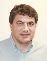 Franck Petit合作论文数CNRS, Université de Picardie Jules Verne2D. Ohebsian合作论文数2Dominique Sarti合作论文数2M. Lemiti合作论文数1f cocco合作论文数1Z Zakrzewski合作论文数1A Grimaud合作论文数1
 Isabel Santiago合作论文数Department of Computer Architecture, Electronic and Electronic Technology., University of Córdoba. Campus de Rabanales;rdoba;c;Department of Computer Architecture, Electronic and Electronic Technology., University of Córdoba1Hassler, C.合作论文数1Laugier, A.合作论文数1Stéphane Abanades合作论文数PROMES1
 Jed Kraiem合作论文数1
 Gilles Flamant合作论文数1Y.Q. Tang合作论文数1
 Olivier Chazot合作论文数Université Catholique de Louvain1Anne-Marie Gomes合作论文数1Abdenbi Almi合作论文数1
 Wilhelm Warta合作论文数Fraunhofer Institute for Solar Energy Systems1Bernard Pateyron合作论文数1J G Lacombe合作论文数1J. Jarosz合作论文数1Daniel J Gauthier合作论文数1
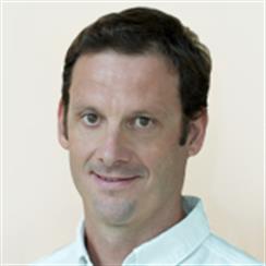 Stefaan De Wolf合作论文数Physical Sciences and Engineering Division, King Abdullah University of Science and Technology1
 Jeanfrancois Coudert合作论文数1
 André Denat合作论文数1




