The effect of solvent vapor annealing on the fluorescence properties and morphology of titanyl phthalocyanine/ perylene phenethylimide thin-film molecular semiconductor bilayers (TiOPc/PPEI) is investigated. A combination of atomic force microscopy (AFM) and near-field scanning optical microscopy (NSOM) is used in conjunction with bulk absorption and fluorescence measurements to correlate the morphological and photophysical properties of these bilayer systems. AFM data show that treatment of the vacuum-deposited amorphous PPEI and TiOPc/PPEI films results in the crystalline transformation of these materials and severely alters the contact between the TiOPc and PPEI layers. AFM data show extended solvent vapor annealing produces void spaces in the TiOPc coverage on the order of several hundred nanometers. Steady-state fluorescence intensity and fluorescence lifetime measurements are used as a measure of charge-transfer quenching efficiencies. Very efficient charge-transfer quenching is observed when amorphous layers of TiOPc are deposited onto PPEI resulting from uniform contact between the layers. Extended annealing results in decreased charge-transfer quenching efficiencies as a result of widely dispersed, localized interfacial contact points.
An improved, cryogenic shadowed evaporation technique has been developed to produce ultra-narrow metallic wires. It has been used to create wires of Pd with widths less than 15 nm and as long as 800 nm. Arrays of wires covering areas as large as 6400 μm2 have been made. This method, which can be extended to other materials and structures, is presently limited by the grain size of the ‘‘template’’ material, and therefore holds promise for even finer linewidths.
 David M. Adams合作论文数1michael j rooks合作论文数1
 Michelle Arkin合作论文数Department of Pharmaceutical Chemistry, School of Pharmacy, University of California, San Francisco1
 Brian Gregg合作论文数Center for Chemistry and Nanoscience, National Renewable Energy Laboratory1
 John Conboy合作论文数Department of Chemistry, University of Oregon1Josef Kerimo合作论文数1
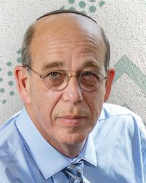 Arie Zaban合作论文数Chemistry Department, Bar-Ilan University1
 Allen Goldman合作论文数School of Physics and Astronomy, College of Science and Engineering, University of Minnesota1Aldo Hoermann合作论文数1
 Gabe Spalding合作论文数Department of Physics, Illinois Wesleyan University;Laboratory for Mesoscopics and Quantum Microscopies, Illinois Wesleyan University1Eric D. A. Stemp合作论文数1
 Jacqueline K. Barton合作论文数Division of Chemistry and Chemical Engineering, California Institute of Technology1




