We report on transport characteristics of field effect two-dimensional electron gases (2DEGs) in 24 nm wide indium arsenide surface quantum wells. High quality single-subband magnetotransport with clear quantized integer quantum Hall plateaus is observed to filling factor ν = 2 in magnetic fields of up to B = 18 T, at electron densities up to 8 ×10¹¹/cm2. Peak mobility is 11 000 cm2/Vs at 2 ×10¹²/cm2. Large Rashba spin–orbit coefficients up to 124 meV Å are obtained through weak anti-localization measurements. Proximitized superconductivity is demonstrated in Nb-based superconductor-normal-superconductor (SNS) junctions, yielding 78%–99% interface transparencies from superconducting contacts fabricated ex situ (post-growth), using two commonly used experimental techniques for measuring transparencies. These transparencies are on a par with those reported for epitaxially grown superconductors. These SNS junctions show characteristic voltages IcRn up to 870 μV and critical current densities up to 9.6 μA/μm, among the largest values reported for Nb-InAs SNS devices.
Among superconductor/semiconductor hybrid structures, in situ aluminum (Al) grown on InGaAs/InAs is widely pursued for the experimental realization of Majorana Zero Mode quasiparticles. This is due to the high carrier mobility, low effective mass, and large Landé g-factor of InAs, coupled with the relatively high value of the in-plane critical magnetic field in thin Al films. However, growing a thin, continuous Al layer using the molecular beam epitaxy (MBE) is challenging due to aluminum's high surface mobility and tendency for 3D nucleation on semiconductor surfaces. A study of epitaxial Al thin film growth on In0.75Ga0.25As with MBE is presented, focusing on the effects of the Al growth rate and substrate temperature on the nucleation of Al layers. We find that for low deposition rates, 0.1 and 0.5 Å/s, the growth continues in 3D mode during the deposition of the nominal 100 Å of Al, resulting in isolated Al islands. However, for growth rates of 1.5 Å/s and above, the 3D growth mode quickly transitions into island coalescence, leading to a uniform 2D Al layer. Moreover, this transition is very abrupt, happening over an Al flux increase of less than 1%. We discuss the growth mechanisms explaining these observations. The results give new insights into the kinetics of Al deposition and show that with sufficiently high Al flux, a 2D growth on substrates at close to room temperature can be achieved already within the first few Al monolayers. This eliminates the need for complex cryogenic substrate cooling and paves the way for the development of high-quality superconductor-semiconductor interfaces in standard MBE systems.
We report on transport characteristics of field effect two-dimensional electron gases (2DEGs) in surface indium antimonide quantum wells. The topmost 5 nm of the 30 nm wide quantum well is doped and shown to promote the formation of reliable, low resistance Ohmic contacts to surface InSb 2DEGs. High quality single-subband magnetotransport with clear quantized integer quantum Hall plateaus is observed to filling factor nu = 1 in magnetic fields of up to B = 18 T. We show that the electron density is gate-tunable, reproducible, and stable from pinch-off to 4 x 10(11) cm(-2), and peak mobilities exceed 24 000 cm(2)/Vs. Large Rashba spin-orbit coefficients up to 110meV . angstrom are obtained through weak anti-localization measurements. An effective mass of 0.019m(e) is determined from temperature-dependent magnetoresistance measurements, and a g-factor of 41 at a density of 3.6 x 10(11) cm(-2) is obtained from coincidence measurements in tilted magnetic fields. By comparing two heterostructures with and without a delta-doped layer beneath the quantum well, we find that the carrier density is stable with time when doping in the ternary Al0.1In0.9Sb barrier is not present. Finally, the effect of modulation doping on structural asymmetry between the two heterostructures is characterized.
The research reported in this publication was supported by King Abdullah University of Science & Technology (KAUST) with Grants No. CRF-2015-SENSORS-2708 and No. URF-2015-2549 and by the Natural Sciences and Engineering Research Council of Canada (NSERC) Discovery Grant No. RGPIN-04178, the Ontario Early Researcher Award, and the Canada First Research Excellence Fund.
We conduct a comprehensive study of three different magnetic semiconductors, CrI3, CrBr3, and CrCl3, by incorporating both few-layer and bilayer samples in van der Waals tunnel junctions. We find that the interlayer magnetic ordering, exchange gap, magnetic anisotropy, and magnon excitations evolve systematically with changing halogen atom. By fitting to a spin wave theory that accounts for nearest-neighbor exchange interactions, we are able to further determine a simple spin Hamiltonian describing all three systems. These results extend the 2D magnetism platform to Ising, Heisenberg, and XY spin classes in a single material family. Using magneto-optical measurements, we additionally demonstrate that ferromagnetism can be stabilized down to monolayer in more isotropic CrBr3, with transition temperature still close to that of the bulk.
We describe an experimental protocol to characterize magnetic field dependent microwave losses in superconducting niobium microstrip resonators. Our approach provides a unified view that covers two well-known magnetic field dependent loss mechanisms: quasiparticle generation and vortex motion. We find that quasiparticle generation is the dominant loss mechanism for parallel magnetic fields. For perpendicular fields, the dominant loss mechanism is vortex motion or switches from quasiparticle generation to vortex motion, depending on cooling procedures. In particular, we introduce a plot of the quality factor versus the resonance frequency as a general method for identifying the dominant loss mechanism. We calculate the expected resonance frequency and the quality factor as a function of the magnetic field by modeling the complex resistivity. Key parameters characterizing microwave loss are estimated from comparisons of the observed and expected resonator properties. Based on these key parameters, we find a niobium resonator whose thickness is similar to its penetration depth is the best choice for X-band electron spin resonance applications. Finally, we detect partial release of the Meissner current at the vortex penetration field, suggesting that the interaction between vortices and the Meissner current near the edges is essential to understand the magnetic field dependence of the resonator properties.
The surface states of a topological insulator (TI) can be induced with superconductivity through proximity with a conventional s-wave superconductor (S). To study the coupling between two superconducting TI surfaces, we report the growth and fabrication of vertical Josephson junctions with the topological insulators (Bi0.5Sb0.5)(2)Te-3 sandwiched between Nb electrodes. We observed two Josephson critical currents on the I-V characteristic at 3.5 K, attributed to the bulk Nb and the proximity-induced superconducting (Bi0.5Sb0.5)(2)Te-3 surfaces, respectively. The enhancement of conductance at these two critical currents leads to a bump and a plateau on the differential conductance spectroscopy. By further cooling down to 300 mK, a zero bias conductance peak (ZBCP) appears on the plateau, which is taken as a feature from the unconventional paring at the (Bi0.5Sb0.5)(2)Te-3-Nb interface.
We use both classical magnetotransport and quantum oscillation measurements to study the thickness evolution of the extremely large magnetoresistance (XMR) material and type-II Weyl semimetal candidate gamma-MoTe2, protected from oxidation. We find that the magnetoresistance is systematically suppressed with reduced thickness. This occurs concomitantly with both a decrease in carrier mobility and increase in electron-hole imbalance. We model the two effects separately and conclude that the XMR effect is more sensitive to the former.
 Guo-Xing Miao (苗国杰)合作论文数Department of Electrical and Computer Engineering, University of Waterloo;Institute for Quantum Computing, University of Waterloo8
 David G. Cory合作论文数Department of Chemistry, University of Waterloo7
 Francois Sfigakis合作论文数Institute for Quantum Computing, University of Waterloo;Department of Chemistry, University of Waterloo5
 Adam W. Tsen合作论文数School of Applied and Engineering Physics,4
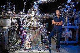 Deler Langenberg合作论文数4
 Ahmed Elbaroudy合作论文数3
 Shazhou Zhong合作论文数Univ Waterloo, Inst Quantum Comp, Waterloo, ON N2L 3G1, Canada3
 Xiaodong Ma合作论文数Medtronic Brain and Spine Therapies3
 Lin Li (李林)合作论文数3Kwon Sangil合作论文数3
 Jonathan Baugh合作论文数Institute for Quantum Computing;University of Waterloo;Institute for Quantum Computing, University of Waterloo3
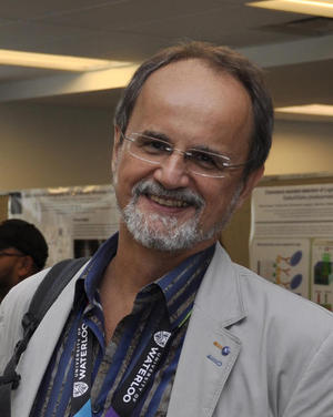 Zbigniew Wasilewski合作论文数Department of Physics and Astronomy, University of Waterloo3E. Annelise Bergeron合作论文数2Ivar Taminiau合作论文数2Shinyoung Lee合作论文数2Anita Fadavi Roudsari合作论文数2Archana Tiwari合作论文数Univ Waterloo, Inst Quantum Comp, Waterloo, ON N2L 3G1, Canada2
 Li Chenghe合作论文数Renmin Univ China, Dept Phys, Beijing 100872, Peoples R China2
 Bowen Yang合作论文数Angstrom Lab, Uppsala Univ2Shangjie Tian合作论文数Renmin Univ China, Dept Phys, Beijing 100872, Peoples R China2
 Long Cheng (程龙)合作论文数School of Physics & Electronics, Hunan University2Benningshof, O.W.B.合作论文数2Yong-Chao Tang合作论文数2
 Kim Hyun Ho合作论文数Dept Chem Engn, Pohang Univ Sci & Technol2
 Fangchu Chen合作论文数Hefei National Laboratory for Physical Sciences at Microscale, University of Science and Technology of China2
 Hechang Lei (雷和畅)合作论文数School of Physics, Renmin University of China2
 Hui Zhang (张汇)合作论文数Low-dimensional Material UHV-Cluster System Laboratory, University of Science and Technology of China;Hefei National Research Center for Physical Sciences at the Microscale, University of Science and Technology of China2
 Xuan Luo (罗轩)合作论文数Institute of Solid State Physics, Hefei Institutes of Physical Science, Chinese Academy of Sciences2Hamid Reza Mohebbi合作论文数Dept . of ECE;Univ . of Waterloo Waterloo;Dept . of ECE, Univ . of Waterloo Waterloo2Sean M. Walker合作论文数1Peter Sprenger合作论文数1
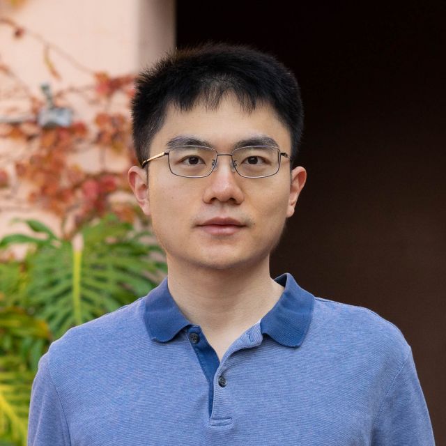 Chenhao Jin合作论文数Department of Physics, University of California, Santa Barbara1Man Chun Tam合作论文数1Zui Tao合作论文数1Yutong Dai合作论文数1
 Liuyan Zhao (赵刘燕)合作论文数Department of Physics, College of Literature, Science, and the Arts, University of Michigan;Quantum Research Institute, University of Michigan1
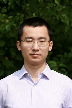 Kai Sun合作论文数College of Literature, Science, and the Arts, University of Michigan-Ann Arbor1
 Kin Fai Mak合作论文数Department of Physics, College of Arts and Sciences, Cornell University1
 Yuping Sun (孙玉平)合作论文数中国科学院合肥物质科学研究院1
 Yan Wen合作论文数1
 Peng Li (李鹏)合作论文数School of Integrated Circuits, University of Science and Technology of China1
 Siwen Li合作论文数University of Michigan1
 Xixiang Zhang合作论文数Physical Science and Engineering Division, King Abdullah University of Science and Technology1
 Shengwei Jiang (姜生伟)合作论文数Institute of Condensed Matter Physics, School of Physics and Astronomy, Shanghai Jiao Tong University1Cheng Long合作论文数1
 Changgan Zeng (曾长淦)合作论文数中国科学技术大学合肥微尺度物质科学国家研究中心/School of Physical Sciences, University of Science and Technology of China1
 Jie Shan合作论文数School of Applied and Engineering Physics, Cornell University1Philip Klipstein合作论文数Optronics Systems Division1
 Chenhui Zhang (张晨辉)合作论文数Department of Mechanical Engineering, Tsinghua University1




