Vertically injected thin-film ultraviolet light-emitting diodes operating at 325 and 280nm are demonstrated. Low-temperature AlN interlayers allow crack-free growth of AlxGa1−xN with compositions up to x=0.53 on GaN-on-sapphire templates. The GaN layer allows laser-induced separation of the highly strained epi stack from the sapphire substrate with high yield. Cathode contacts are formed on nitrogen-face AlxGa1−xN (up to x=0.53) and allow vertical injection of current into the active region. Controlled roughening of the nitrogen-face AlxGa1−xN is also demonstrated through photoelectrochemical etching and results in >2.5× light extraction gain for 325 and 280nm devices.
Data are presented on the operation of thin-film flip-chip InGaN/GaN multiple-quantum-well light-emitting diodes (LEDs). The combination of thin-film LED concept with flip-chip technology is shown to provide surface brightness and flux output advantages over conventional flip-chip and vertical-injection thin-film LEDs. Performance characteristics of blue, white, and green thin-film flip-chip 1x1 mm(2) LEDs are described. Blue (similar to 441 nm) thin-film flip-chip LEDs are demonstrated with radiance of 191 mW/mm(2) sr at 1 A drive, more than two times brighter than conventional flip-chip LEDs. An encapsulated thin-film flip-chip blue LED lamp is shown to have external quantum efficiency of 38% at forward current of 350 mA. A white lamp based on a YAG:Ce phosphor coated device exhibits luminous efficacy of 60 lm/W at 350 mA with peak efficiency of 96 lm/W at 20 mA and luminance of 38 Mcd/m(2) at 1 A drive current. Green (similar to 517 nm) devices exhibit luminance of 37 Mcd/m(2) at 1 A. (c) 2006 American Institute of Physics.
Electrical operation of III-Nitride light emitting diodes (LEDs) with photonic crystal structures is demonstrated. Employing photonic crystal structures in III-Nitride LEDs is a method to increase light extraction efficiency and directionality. The photonic crystal is a triangular lattice formed by dry etching into the III-Nitride LED. A range of lattice constants is considered (a ~ 270 - 340nm). The III-Nitride LED layers include a tunnel junction providing good lateral current spreading without a semi-absorbing metal current spreader as is typically done in conventional III-Nitride LEDs. These photonic crystal III-Nitride LED structures are unique because they allow for carrier recombination and light generation proximal to the photonic crystal (light extraction area) yet displaced from the absorbing metal contact. The photonic crystal Bragg scatters what would have otherwise been guided modes out of the LED, increasing the extraction efficiency. The far-field light radiation patterns are heavily modified compared to the typical III-Nitride LED’s Lambertian output. The photonic crystal affects the light propagation out of the LED surface, and the radiation pattern changes with lattice size. LEDs with photonic crystals are compared to similar III-Nitride LEDs without the photonic crystal in terms of extraction, directionality, and emission spectra.
Electrical operation of InGaN/GaN quantum-well heterostructure photonic crystal light-emitting diodes (PXLEDs) is demonstrated. A triangular lattice photonic crystal is formed by dry etching into the top GaN layer. Light absorption from the metal contact is minimized because the top GaN layers are engineered to provide lateral current spreading, allowing carrier recombination proximal to the photonic crystal yet displaced from the metal contact. The chosen lattice spacing for the photonic crystal causes Bragg scattering of guided modes out of the LED, increasing the extraction efficiency. The far-field radiation patterns of the PXLEDs are heavily modified and display increased radiance, up to ∼1.5 times brighter compared to similar LEDs without the photonic crystal.
Native oxide technology is used to fabricate long wavelength (λ∼1.3 μm) InAlAs-InP-InGaAsP quantum well heterostructure laser diodes with a buried oxide undercutting and constricting the ridge-waveguide active region. The buried native oxide of InAlAs constricts the current and reduces edge and surface losses. Data are presented showing threshold currents as low as ∼140 mA for ∼13-μm-wide stripes (L∼750 μm), with maximum continuous wave output powers as high as ∼225 mW/facet and external differential quantum efficiencies up to 67% (300 K, uncoated facets).
 Mike Krames合作论文数Arkesso LLC;Opnovix Corp.14
 Jonathan Wierer合作论文数Department of Electrical and Computer Engineering, College of Engineering, North Carolina State University7
 Nathan Gardner合作论文数LumiLeds Lighting6
 Oleg B. Shchekin合作论文数Advanced Laboratories, Philips Lumileds Lighting Company4
 Paul S Martin合作论文数3Daniel A. Steigerwald合作论文数3Gerard Harbers合作论文数3mark pugh合作论文数2
 Mihail Sigalas合作论文数Department of Materials Science, University of Patras2Joel R. Wendt合作论文数2Serge J. Bierhuizen合作论文数2Tal Margalith合作论文数2
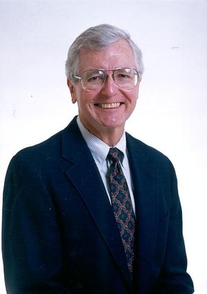 M. George Craford合作论文数Philips Lumileds Lighting Company2grigoriy basin合作论文数1gregory w eng合作论文数1zhuoxiang ren合作论文数1Melvin McLaurin合作论文数1w goetz合作论文数1Herbert P. Schweizer合作论文数1Holcomb, M.O.合作论文数1
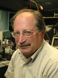 Steven R. J. Brueck合作论文数Center for High Technology Materials, University of New Mexico;Physics & Astronomy Department, University of New Mexico;School of Engineering, University of New Mexico1
 Stefano Schiaffino合作论文数Venetian Institute of Molecular Medicine (VIMM), Padova1
 Jung Han合作论文数School of Engineering & Applied Science, Yale University1
 Michael Kneissl合作论文数Institute of Solid State Physics, Faculty II – Mathematics and Natural Sciences, Technische Universität Berlin;Ferdinand-Braun-Institut, Leibniz-Institut für Höchstfrequenztechnik1M. Shagam合作论文数1Dong Li合作论文数1
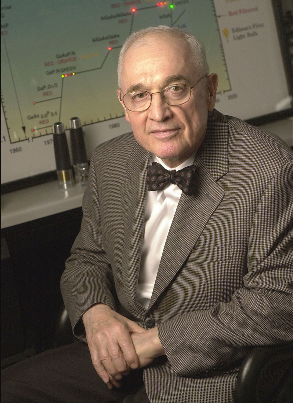 Nick Holonyak合作论文数Holonyak Micro & Nanotechnology Lab, The Grainger College of Engineering, University of Illinois at Urbana-Champaign1N.M. Johnson合作论文数1
 A. A. Allerman合作论文数Advanced Electronic and Optoelectronic Materials Department, Sandia National Laboratories1Troy Trottier合作论文数1Regina Mueller-Mach合作论文数Electroluminescent Technology Department, Hewlett Packard Laboratories1
 Maria Gherasimova合作论文数Department of Materials Science and Engineering, University of Virginia1Gerd O. Mueller合作论文数1




