We show that N-doped ZnO films grown on sapphire can exhibit significant (∼1018 cm−3) room-temperature p-type behavior when sufficient nitrogen (N) is incorporated and the material is annealed appropriately. Substitutional N on the oxygen (O) sublattice is a deep acceptor; however, shallow acceptor complexes involve N, H, and zinc vacancies (VZn). Combining secondary ion mass spectrometry, Raman-scattering, photoluminescence, and Hall-effect data, we establish the evolution of N from its initial incorporation on a Zn site to a final shallow acceptor complex VZn_NO_H+ with an ionization energy of ca. 130 meV. This complex is responsible for the observed p-type behavior.
We find that surface second-harmonic generation (SHG) from epitaxial graphene on a vicinal SiC(0001) substrate is enhanced ~25% by direct electric current in graphene and that the enhanced SHG varies strongly with the measurement location.
We find that the flow of direct electric current (dc) through graphene on substrate enhances surface optical second-harmonic generation (SHG) from the graphene/substrate system. The current can enhance surface SHG by about 300% for a chemical-vapor-deposition (CVD) graphene monolayer on a SiO${}_{2}/\mathrm{Si}(001)$ substrate, and by about 25% for an epitaxial four-layer-graphene film on a 3.5\ifmmode^\circ\else\textdegree\fi{}-miscut vicinal SiC(0001) substrate. The enhancement in both the CVD and epitaxial graphene samples is due to electric field-induced SHG, which is produced by the current-associated vertical electric field at the SiO${}_{2}/$Si interface or at the graphene/SiC interface. Measurements of rotational-anisotropy SHG (RA-SH) from both samples revealed that the current-induced SHG varies strongly with the measurement location along the current flow direction. By measuring RA-SH from the vicinal SiC(0001) substrate, we determined all three second-order susceptibility tensor elements (${d}_{33}$ = \ensuremath{-}52.0 pm/V, ${d}_{15}$ = 20.0 pm/V, and ${d}_{31}$ = 18.7 pm/V) that characterize the SHG response of hexagonal SiC at the fundamental wavelength of 740 nm. We further determined the three effective susceptibility tensor elements (${d}_{33}$ = \ensuremath{-}135.8 pm/V, ${d}_{15}$ = 18.5 pm/V, and ${d}_{31}$ = 14.6 pm/V) that characterize the surface SHG from the graphene/vicinal-SiC(0001) sample and finally showed that the current-dependent tensor element ${d}_{33}$ can be enhanced to a large value of ${d}_{33}$ = \ensuremath{-}199.0 pm/V by electric current in epitaxial graphene.
Iron phthalocyanine adsorbed on an oxygen covered Fe(110) surface shows a complex coverage-dependent spin polarization during growth of a molecular monolayer. Spin polarization is modified at low submonolayer coverages, absent at intermediate submonolayer coverages, and reappears in modified form for a complete monolayer. This is attributed to coverage-dependent adsorption configurations from a random adsorption system to a packed monolayer with a well-defined interfacial spin polarization. In addition, we report on the observation of a rotation of the spin direction of photoelectrons in the presence of molecules which is attributed to molecular modifications of surface magnetic anisotropy.
We present a novel technique of growing UHV graphene using atomic hydrogen etching of SiC(0001)–Si surfaces. Hydrogen atoms generated from a hot tungsten filament selectively etch silicon surface atoms thereby facilitating the Si-sublimation process at temperatures around 1000°C according to Auger Electron Spectroscopy. This allows for separate, non-thermal control of the rate of formation of the interfacial buffer layer formation to yield reduced pit formation observed by scanning tunneling microscopy during subsequent UHV graphene growth.
We show using scanning tunneling microscopy, spectroscopy, and ab initio calculations that several intercalation structures exist for Na in epitaxial graphene on SiC(0001). Intercalation takes place at room temperature and Na electron-dopes the graphene. It intercalates in-between single-layer graphene and the carbon-rich interfacial layer. It also penetrates beneath the interfacial layer and decouples it to form a second graphene layer. This decoupling is accelerated by annealing and is verified by direct Na deposition onto the interface layer. Our observations show that intercalation in graphene is fundamentally different than in graphite and is a versatile means of electronic control.
We discuss Extended X-ray Absorption Fine Structure (EXAFS) experiments on impurities in semiconductors. The local structure of the impurity site is determined for the first, second and third neighbor shells. These studies are carried out on absorption edges in the soft x-ray region using a novel fluorescence detection scheme which reveals improved detection sensitivity when compared with more standard electron Auger yield methods. The higher detection sensitivity allows structural studies at atomic densities as low as 1018 at/cm3 and this technique is used to study the local structure of P and S impurities in GaAs and of S in AlxGa1-xAs at concentrations of 1019–1020 at/cm3. The P atoms are substitutional on As sites, and a breathing relaxation of the P first shell Ga atoms is responsible for a P-Ga distance of 2.38A, which is 0.07A shorter than the As-Ga distance in GaAs(2.45A). No detectable relaxation is observed in the P second and third atomic shells. In Sdoped GaAs we find two different populations of S-Ga bonds with nearly equal intensity and both with S located on the As sub-lattice. These findings indicate two different configurations of substitutional S in GaAs. The coexistence of two similarly populated, charge compensating configurations is the first structural evidence which allows us to explain the observation that in n-doped GaAs the electrical activity of donors is lower than the atomic concentration. Finally, we present experimental results on S impurities in AlxGa1-xAs (0.2<x<0.5). In this system, at the Al concentrations we studied, the S impurities are bound only to Al and not to Ga atoms. We report the formation of an extended complex which is discussed in connection with the structural identification of DX centers in these materials.
We have investigated the (0001) surfaces of several hexagonal manganite perovskites by low-energy electron diffraction (LEED) in order to determine if the surface periodicity is different from that of the bulk materials. These LEED studies were conducted using near-normal incidence geometry with a low energy electron microscope (LEEM)/LEED apparatus from room temperature to 1200 degrees C and with an electron energy in the range of 15-50 eV. Diffraction patterns showed features of bulk-terminated periodicity as well as a 2 x 2 surface reconstruction. Possible origins for this surface reconstruction structure are discussed and comparisons are made with surface studies of other complex oxides.
Titanium silicide islands have been formed by the ultrahigh vacuum deposition of thin films of titanium (< 2 nm) on atomically clean Si(100) substrates followed by annealing to ~800 degrees C. Scanning tunneling microscopy (STM) and scanning tunneling spectroscopy have been performed on these islands to record current-voltage (I-V) curves. Because each island forms a double barrier tunnel junction (DBTJ) structure with the STM tip and the substrate, they would be expected to exhibit single electron tunneling (SET) according to the orthodox model of SET. Some of the islands formed are small enough (diameter < 10 nm) to exhibit SET at room temperature and evidence of SET has been identified in some of the I-V curves recorded from these small islands. Those curves are analyzed within the framework of the orthodox model and are found to be consistent with that model, except for slight discrepancies of the shape of the I-V curves at current steps. However, most islands that were expected to exhibit SET did not do so, and the reasons for the absence of observable SET are evaluated. The most likely reasons for the absence of SET are determined to be a wide depletion region in the substrate and Schottky barrier lowering due to Fermi level pinning by surface states of the clean silicon near the islands. The results establish that although the Schottky barrier can act as an effective tunnel junction in a DBTJ structure, the islands may be unreliable in future nanoelectronic devices. Therefore, methods are discussed to improve the reliability of future devices.
 Giorgio Margaritondo合作论文数EPFL37
 SB CHRISTMAN合作论文数36
 Theodore E. Madey合作论文数Rutgers University29
 Gunther Klaus Wertheim合作论文数Light Source Division, National Synchrotron Radiation Research Center22P. H. Citrin合作论文数18Ee Chaban合作论文数14andreas sandin合作论文数14M. D. Ulrich合作论文数13
 Daniel B. Dougherty合作论文数University of Pittsburgh, University of Pittsburgh12
 Jeff Keister合作论文数11Jm Poate合作论文数10Jj Kolodziej合作论文数10D.N.E. Buchanan合作论文数9Neville V Smith合作论文数9
 Yves Chabal合作论文数Erik Jonsson School of Engineering and Computer Science, University of Texas Dallas9
 Francesco Sette合作论文数European Synchrotron Radiation Facility9Sp Weeks合作论文数8Michael Schluter合作论文数8Harald Ibach合作论文数8A.S.Y. Chan合作论文数7Christma.Sb合作论文数7
 Gerald Lucovsky合作论文数Department of Physics, North Carolina State University7Kl Shaklee合作论文数6DA ZWEMER合作论文数6
 Manuel Cardona合作论文数Department of Solid State Spectroscopy, Max Planck Institute for Solid State Research6R.A. Malic合作论文数6m m traum合作论文数5H. Niimi合作论文数5
 Stephen J. Pearton合作论文数Department of Materials Science and Engineering, Herbert Wertheim College of Engineering, University of Florida5
 John M. Poate合作论文数Colorado School of Mines5
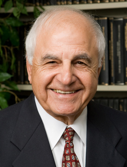 George Haddad合作论文数Department of Electrical Engineering and Computer Science, The University of Michigan5Maurice Campagna合作论文数5
 Peter Michael Eisenberger合作论文数5D Mark Riffe合作论文数5
 Charles Shank合作论文数Lawrence Berkeley National Laboratory;Department of Physics, University of California, Berkeley5C. A. Crider合作论文数5
 David Aspnes合作论文数Department of Physics and Astronomy, College of Sciences, North Carolina State University5Tt Sheng合作论文数4Konrad, G. T.合作论文数4Ernst Bucher合作论文数Solarforschungsinstitut ISC4C.-M. Chiang合作论文数4
 Robert Nemanich合作论文数Department of Physics, Arizona State University4H. Kasper合作论文数4C. T. Chen合作论文数4Michael J Gladys合作论文数4
 Christopher Wiebe合作论文数Department of Chemistry, University of Winnipeg;Department of Physics and Astronomy, McMaster University4D. R. Hamann合作论文数4
 Alain C. Diebold合作论文数Department of Nanoscale Science & Engineering, College of Nanotechnology, Science, and Engineering, University at Albany, State University of New York;Center of Nanoscale Metrology, University at Albany, State University of New York4PA BENNETT合作论文数3




