Structures of concentric microdisk and rings were studied theoretically and experimentally. A three-dimensional (3-D) model was developed, emphasizing the possibility of coupling several concentric microresonators. The 3-D analysis resulted in closed-form analytic expressions for the six field components from which the limitations and necessary conditions for concentric coupling were derived. We emphasized the important differences between our results and the predictions of the more commonly used two-dimensional models-the latter are failing to predict the concentric coupling actual feasibility. Finally, we present experimental results of coupled ring vertical-cavity surface-emitting lasers, revealing a good match to the 3-D model predictions.
Coupling between whispering-gallery modes of concentric microcavity lasers was analyzed, and a closed-form three-dimensional vectorial solution for the coupled fields was obtained. Experiments performed with concentric gain-guided vertical cavity ring lasers resulted in regimes of resonant coupling in good agreement with the theory.
calculated dependency of IVBA on the hole density being in very good agreement with absorption measurements on p-GaAs.',' At T = 300 K andp = 10" ~ m ~ , the calculated IVBA coefficients of GaAs are a(1.55 pm) = 33 cm-' with dddp(1.55 pm) = 3.4 X ~ m ~ a n d a ( 1 . 3 pm) = 16cm-'withda/dp(l.3 pm) = 1.6 X cm2. The temperature dependency will be discussed. Free carrier absorption (intraband transitions within one vamagnitude at A = 1.55 pm. Figure 2 shows the WEDNESDAY AFTERNOON / CLE0'97 / 235
A methodology for calculating the energy band diagrams of abrupt heterostructures using the band discontinuities and the interface charge density as parameters is presented. The calculations are based on two basic equations which are universally accepted—the lineup of the bands relative to the common Fermi level (which embodies the valence band discontinuity) and the charge neutrality (which embodies the interface charge density). The two equations, with the aid of Poisson's equation, yield the total band bending on each side of the interface and the dependence of the energy bands on the position (i.e. the band diagram). The methodology is illustrated for the HgTeCdTe semimetal-semiconductor heterostructure, and demonstrates the interplay of band offsets and interface charges in establishing the nature of a heterostructure (either rectifying or ohmic) and in determining the potential barrier height, for both n-type and p-type CdTe. The methodology presented in this study is general and can be applied to additional semiconductor-semiconductor and semimetal-semiconductor heterostructures.
Large circular VCSELs exhibit spontaneous transition from vertical to almost in-plane, quasi whispering gallery lasing modes. Enhancing this effect by coupling to concentric ring VCSELs is demonstrated and analyzed.
CdTe epilayers are grown by metalorganic chemical vapor deposition (MOCVD) on bulk HgCdTe crystals with x ~ 0.22 grown by the traveling heater method (THM). The THM HgCdTe substrates are (111) oriented and the CdTe is grown on the Te face. The metalorganic sources are DMCd and DETe, and the growth is performed at subatmospheric pressure. Ultraviolet (UV) photon-assisted hydrogen radicals pretreatment plays a dominant role in the electrical properties of the resulting heterostructures. The requirements of a good passivation for HgCdTe photodiodes vis-a-vis the passivation features of CdTe/HgCdTe heterostructures are discussed. The effect of valence band offset and interface charges on the band diagrams of p-isotype CdTe/HgCdTe heterostructures, for typical doping levels of the bulk HgCdTe substrates and the MOCVD grown CdTe, is presented. Electrical properties of the CdTe/HgCdTe passivation are determined by capacitance-voltage and current-voltage characteristics of metal-insulator-semiconductor test devices, where the MOCVD CdTe is the insulator. It is found that the HgCdTe surface is strongly inverted and the interface charge density is of the order of 1012cm2 when the CdTe epilayer is grown without the UV pretreatment. With the in-situ UV photon-assisted hydrogen radicals pretreatment, the HgCdTe surface is accumulated and the interface charge density is -4. 1011 cm-2.
The energy-band diagram and interface potentials at a HgTe-CdTe abrupt heterostructure are presented. An analytic approximation is formulated and compared to an exact (numeric) calculation of the interface potentials. The error introduced by the analytic approximation is negligible for a wide range of doping levels of the CdTe. The analysis predicts that HgTe forms ohmic contacts to p-type CdTe and rectifying junctions to n-type CdTe. Interface charges above 1012 cm−2 modify the interface potentials. Positive interface charge imposes depletion in p-type CdTe resulting in potential barriers that may degrade the ohmic properties of the contacts. The methodology presented in this study may be extended to additional semimetal-semiconductor heterostructures.
A novel chip implementing real-time image convolution features a pure bit-serial architecture and systolic array structure. It consists of a 3*3 array of modular units that can be easily enlarged. The basic unit heart is a very efficient bidirectional multiplier, which can perform two different multiplications simultaneously. The chip overall size is 5.78 mm * 3.18 mm (in CMOS 2 mu technology). It is full-precision and has a throughput of one 20 bit convolution every 10 clock cycles, with a latency of 24 clock cycles.<>
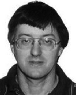 Meir Orenstein合作论文数4
 Yael Nemirovsky合作论文数Faculty of Electrical Engineering, Technion – Israel Institute of Technology;TODOS Technologies Ltd.3
 David Arbel合作论文数Micro-Photonics Lab .;Electrical Engineering Dept;Technion - Israel Institute of Technology2
 David Goren合作论文数1Noa Amir合作论文数1
 Ran Ginosar合作论文数The Andrew & Erna Viterbi Faculty of Electrical Engineering, Technion-Israel Institute of Technology;VLSI Systems Research Center, Technion-Israel Institute of Technology;Advanced Circuit Research Center, Technion-Israel Institute of Technology;Technion Computer Engineering Center, Technion-Israel Institute of Technology1




