Existing computational spectral imaging systems typically rely on coded aperture and beam splitters that block a substantial fraction of incident light, degrading reconstruction quality under light-starved conditions. To address this limitation, we develop the Oscillating Dispersion Imaging Spectrometer (ODIS), which for the first time achieves near-full light throughput by axially translating a disperser between the conjugate image plane and a defocused position, sequentially capturing a panchromatic (PAN) image and a dispersed measurement along a single optical path. We further propose a PAN-guided Dispersion-Aware Deep Unfolding Network (PDAUN) that recovers high-fidelity spectral information from maskless dispersion under PAN structural guidance. Its data-fidelity step derives an FFT-Woodbury preconditioned solver by exploiting the cyclic-convolution property of the ODIS forward model, while a Dispersion-Aware Deformable Convolution module (DADC) corrects sub-pixel spectral misalignment using PAN features. Experiments show state-of-the-art performance on standard benchmarks, and cross-system comparisons confirm that ODIS yields decisive gains under low illumination. High-fidelity reconstruction is validated on a physical prototype.
Objective The pursuit of high-efficiency, ultra-thin optical absorbers is an important goal in modern photonics, with key applications in solar energy harvesting, photodetection, thermal emission, and stealth technology. Metasurfaces-planar arrays of subwavelength nanostructures-have become a versatile platform for manipulating light-matter interactions, enabling near-perfect absorption via tailored electromagnetic resonances including guided-mode resonances (GMRs) and surface plasmon polaritons (SPPs). However, conventional metasurface absorbers typically suffer from distinct spectral dips across broadband wavelengths due to their discrete resonant modes, which significantly lower the overall average absorption. Consequently, there is a strong demand for innovative design strategies that improve broadband absorption without sacrificing structural simplicity or degrading existing absorption peaks. This work addresses the above limitation by proposing and demonstrating a new pixelated hybrid metasurface design. We integrate two different periodic lattices into a single planar metasurface to form a multi-periodic supercell. The goal is to exploit the complementary spectral responses of the two lattices, such that the absorption valleys of one lattice coincide with the absorption peaks of the other, thereby filling the spectral dips and achieving a smooth, enhanced broadband absorption profile from 0.4 & micro;m to 1.8 & micro;m, a range highly relevant for solar and infrared applications. Methods A multilayer metasurface absorber is systematically designed, consisting of a SiO2 substrate, a periodic array of photoresist (PR) nanocylinders, and a functional thin-film stack of titanium nitride (TiN), nickel (Ni), and silicon nitride (Si3N4). TiN is used as a lossy plasmonic layer, Ni serves as an optically opaque bottom layer to suppress transmission, and Si3N4 acts as a dielectric spacer to support guided-mode resonances. Numerical simulations and optimizations are performed using the finite-difference time-domain (FDTD) method. The effects of key structural parameters are investigated in detail, including the thicknesses of the Si3N4 (h1), Ni (h2), and TiN (h3) layers, the height of PR nanocylinders (h4), the lattice duty cycle ( f ), and the angle of incidence. The optimization target is to maximize the average absorption in 0.4-1.8 & micro;m for a baseline single-period structure. After parametric scanning, it is found that lattices with periods of 430 nm and 550 nm exhibit strongly complementary absorption spectra: the absorption valleys of one structure correspond well to the absorption peaks of the other. Based on this observation, a pixelated hybrid metasurface is designed by interleaving 430 nm and 550 nm unit cells in a 1:1 spatial pattern. Samples are fabricated using frequency-tuned interference lithography to define the PR nanocylinders, followed by thin-film deposition (e.g., sputtering) of TiN, Ni, and Si3N4 layers. A reference sample with a uniform 430 nm period is also prepared for comparison. Results and Discussions FDTD simulations show that the optimized single-period (430 nm) structure with h1=165 nm, h2=20 nm, h 3=90 nm, h 4=95 nm, and f=0.4 achieves a simulated average absorption of 79 degrees o and a peak absorption above 98 degrees o in the target band. Electric field distributions at characteristic wavelengths reveal the underlying resonance mechanisms. At 480 nm, strong electric field localization appears at the top surface of Si3N4 and the Ni-Si3N4 interface, indicating the co-excitation of guided-mode resonance and surface plasmon resonance, which jointly produce a strong absorption peak. At 655 nm, the field is mainly confined inside the Si3N4 layer, corresponding to a dominant guided-mode resonance. With increasing period, the second absorption peak and nearby valleys show a clear redshift, confirming the complementary behavior between 430 nm and 550 nm lattices. Experimental results agree well with simulations. The fabricated single-period (430 nm) sample yields an average absorption of 68 degrees o over 0.4-1.8 & micro;m, with a peak absorption of 93 degrees o and obvious dips near 565 nm and 745 nm. The absorption remains stable up to an incident angle of 60 degrees , showing excellent angular insensitivity. In contrast, the pixelated hybrid sample effectively fills the spectral dips without reducing the original peak absorptions. Specifically, the absorption at 645 nm is improved from 65 degrees o to 80 degrees o (an enhancement of 15 percentage points), at 745 nm from 63 degrees o to 73 degrees o (an enhancement of 10 percentage points), and at 830 nm from 53 degrees o to 61 degrees o (an enhancement of 8 percentage points). This leads to a 10-percentage-point enhancement in average absorption across the entire band. These results verify that the 1:1 pixelated combination of 430 nm and 550 nm lattices provides complementary enhancement at spectral valleys, while preserving high peak absorption and thus significantly boosting the device's broadband performance. Conclusions This work proposes, fabricates, and experimentally verifies a novel pixelated variable-period metasurface absorber that greatly enhances broadband optical absorption. We demonstrate that the spectral dip problem in broadband metasurface absorbers can be effectively solved by rationally arranging meta-atoms with complementary resonant responses in the in-plane direction. The core innovation is the pixelated hybridization of 430 nm and 550 nm periodic lattices, which uses mismatched peak - valley positions to achieve synergistic enhancement. The resulting metasurface increases the average absorption by 10 percentage points across 0.4- 1.8 & micro;m, mainly by filling three major dips at 645 nm, 745 nm, and 830 nm. This strategy preserves structural simplicity and an ultra-thin geometry while achieving superior broadband performance. The results highlight spatial multiplexing and pixelation as a general design principle for next-generation photonic meta-devices. Beyond perfect absorption, this approach can be extended to structural color, wavefront shaping, holography, and other functionalities requiring broadband or multiband operation. The demonstrated pixelated metasurface absorber offers a promising route toward high-performance optoelectronic systems for renewable energy, thermal photonics, and infrared sensing.
Glasses-free 3D displays are emerging as a next-generation technology that will redefine interactions with the digital world. One challenge to deliver a truly immersive viewing experience is limited spatial/angular resolution, caused by distributing pixels on the display panel across numerous viewing angles, thereby restricting the display quality of each individual perspective. Here we demonstrate a high-performance glasses-free 3D display with adaptive light field reconstruction through a machine-learning-based design process. This inverse design method, developed using a voxel-based neural network, optimizes a large-scale flat optics element for effective light-field modulation to realize portable 3D displays with arbitrary view distributions. This system enables higher display resolution by increasing the density of views only where users typically focus their attention while reducing density of views in less critical regions to optimize the display quality. With this method, we achieved a 100-mm flat-optics element with 1.5 & times; 1010 phase-modulating subpixels (optical degrees of freedom), far exceeding the pixel count of a 4K panel. We constructed a glasses-free 3D display with a remarkable angular resolution up to 0.67 views per degree by a simple integration with an off-the-shelf purchased liquid crystal display, achieving a two-fold increase in display resolution with smoother motion parallax than conventional systems.
Augmented reality (AR) displays require lightweight, transparent optical combiners, making diffractive waveguides a leading solution. However, achieving both high system optical efficiency and excellent eyebox uniformity remains a fundamental challenge, as these metrics are inherently subject to a trade-off in conventional waveguides based solely on either polarization volume gratings (PVGs) or surface relief gratings (SRGs). To overcome this limitation, we propose a hybrid waveguide architecture that synergistically combines a high-efficiency PVG as the input coupler with a custom-designed two-dimensional SRG (2D-SRG) as the output coupler. The PVG maximizes light injection, while the 2D-SRG enables precise control of out-coupling efficiency at each total internal reflection (TIR) for uniform eyebox illumination. We introduce a k-vector matching error model to quantify fabrication tolerances and guide the design. A 4.65-inch prototype demonstrates an eightfold enhancement in in-coupling diffraction efficiency compared with a conventional SRG-based design. The full system achieves a system optical efficiency of 5% (approximately five times that of a standard all-SRG waveguide) while maintaining an eyebox uniformity of 45%. This work demonstrates a practical co-design strategy that effectively mitigates the intrinsic efficiency-uniformity trade-off, advancing the development of high-performance AR displays.
Enhancing perceptual dimensions while miniaturizing imaging systems presents significant challenges for high-dimensional visual sensing. Conventionally, the acquisition of the 5D (x,y,u,v,λ) spectral light field (5D-SLF) data cube relies on bulky and expensive camera arrays, which are impractical for widespread application. Existing single-detector systems are fundamentally limited by a trade-off between the resolutions of different dimensions owing to insufficient coding capabilities. Here we introduce an Aperture-aware Dispersion Light-field Imaging Spectrometer (ADLIS), that targets a synergy between compactness and resolution through aperture-multiplexed modulation, leveraging the inherent spectral-filtering properties of birefringent material. Using only a manufacturing-friendly and cost-effective phase plate made of birefringent quartz crystal, the aperture of the proposed ADLIS enables compact angular-spectral encoding that is highly sensitive to both the incident angle and spectrum of incoming light. In contrast to the viewpoint-separation approach of microlens arrays, ADLIS employs aperture encoding to superimpose all viewpoints onto each sensor pixel. This shifts the design paradigm from spatial division to encoding integration, aiming to achieve full-resolution light field recovery. Thus, we develop the Aperture-aware Dispersion Light-field Imaging (ADLI) framework, which optimizes the aperture design and 5D-SLF reconstruction in an end-to-end (E2E) manner. Trained by simulation data and validated through real-world experiments, our system achieves robust high-performance 5D-SLF imaging while maintaining full spatial resolution.
We propose and experimentally demonstrate a super-resolution liquid-crystal photoalignment (SPLCP) method based on polarization-induced molecular reorientation and sub-spot mechanical displacement. The molecular orientation angles of photoalignment material SD1 can be reversibly reoriented by ultraviolet (UV) exposure with different linear polarization states, from which the liquid crystal (LC) molecules coated on the SD1 layer are oriented along the long-axis of the SD1 molecules. By combining precise mechanical scanning with sub-spot displacement and UV exposure cycles with tunable linear polarization states, the photoalignment resolution of SD1 layer with a feature size of sub-diffraction limit is achieved, from which a super-resolution planar LC element can be fabricated solely through UV exposure and coating. Therefore, light can be arbitrarily manipulated by the LC element with a designed orientation angle pattern of molecules corresponding to Pancharatnam-Berry phase. A UV pulsed laser with a wavelength of 355 nm, an objective lens with numerical aperture (NA) of 0.8 and a translation stage with sub-spot displacement of 0.2 µm are implemented to construct the exposure system. The minimum linewidth of the fabricated LC element by the proposed SPLCP method achieves 0.2 µm, which is ∼ 0.74 times that of the diffraction limit. Furthermore, a polarization volume grating (PVG) with an aperture of 1 cm, a thickness of 3.9 µm and a period of 1.6 µm is fabricated, in which the first-order diffraction efficiency achieves 93.7% compared with the theoretical efficiency of 100% at the working wavelength of 532 nm. The proposed SPLCP method provides an idea for super-resolution, high-speed and large-scale fabrication of planar and functional optical elements without complicated coating and etching preparation.
In this paper, we propose a fast-switching two-dimensional/three-dimensional (2D/3D) display based on a liquid crystal planar lenticular lens array (LCPLLA) with an ultra-thin functional layer. The LCPLLA enables rapid switching between focusing (3D) and transparent (2D) states through electrical control of the in-plane orientation of liquid crystal (LC) molecules. This design utilizes Pancharatnam-Berry phase principle rather than geometric curvature, thereby significantly reducing the thickness of the LC functional layer. Experimental results demonstrate that the device achieves a total switching time of 14 ms between the 2D and 3D modes, operates at a driving voltage of 8 V, and exhibits uniform focusing with well-defined focal spots, where the focal spot size variation across the lens array is below 1%. At the optimal viewing distance of 370 mm, the system provides high-resolution 2D images and distinct 3D visual effects. The proposed approach offers a compact, high-quality, and fast-responding solution for switchable 2D/3D displays.
Significance Augmented reality (AR) has emerged as a core technology driving the next generation of intelligent human-computer interaction, with diffractive waveguide serving as the pivotal optical component that determines the performance limits of AR devices, such as form factor, field of view (FOV), and display quality. As the demand for lightweight, high-immersion AR glasses surges in consumer electronics, industrial applications, and aerospace fields, traditional optical solutions face insurmountable bottlenecks. The "impossible triangle" of full-color display, large FOV, and monolithic thin design has long constrained the industrialization of AR technology. Diffractive waveguide, leveraging its compatibility with semiconductor manufacturing processes and potential for miniaturization, has become the most promising candidate to break this deadlock. A comprehensive review of its technological evolution, key challenges, and innovative solutions is therefore essential to guide future research directions and promote the integration of AR technology into practical applications. Progress This review systematically elaborates on the research progress of AR optical display and diffractive waveguide technology, covering core structures, optimization strategies, and emerging design methods. In terms of fundamental structures, the optical path principles of mainstream AR display systems are compared, including Birdbath, freeform surface mirror, freeform surface prism, geometric coupling waveguide, diffractive coupling waveguide, and metasurface integrated structures, with their respective advantages and limitations clarified through structural schematics. For diffractive waveguide, the review focuses on 2D exit pupil expansion technology, a critical link to achieving large FOV. Commercial and dual-channel schemes are also discussed, such as Microsoft HoloLens 2's "butterfly-shaped" structure and the dual-channel design, which improve FOV utilization through symmetric grating layouts. In terms of performance optimization, targeted solutions for core challenges such as dispersion, low diffraction efficiency, and uneven brightness are summarized. Various grating structures, including surface relief gratings (SRG) and volume holographic gratings, are analyzed for their ability to balance efficiency and uniformity. The review highlights that the adoption of high-refractive-index materials (e.g., silicon carbide with a refractive index above 2.6) has enabled FOV exceeding 60 degrees , addressing the limitation of traditional glass substrates with refractive indices below 2.0. The review also discusses the emerging AI-driven design method, which revolutionizes the traditional experience-dependent iterative design paradigm. Multiple innovative neural network architectures have been proposed for the inverse design and performance prediction of diffractive waveguide gratings. Conclusions and Prospects Current research on diffractive waveguide has made significant progress in exit pupil expansion, performance optimization, and design methodology, with AI-driven design emerging as a core breakthrough to overcome traditional limitations. However, challenges remain, including residual dispersion in full-color display, insufficient diffraction efficiency in large FOV scenarios, and the need for high-precision manufacturing processes. Future development directions will focus on three aspects: first, the integration of metasurfaces to eliminate dispersion and achieve 100 degrees-120 degrees FOV with monolithic design; second, the deep fusion of AI algorithms with physical models to enhance the interpretability and robustness of design results; and third, the development of high-refractive-index, low-loss materials and compatible large-scale manufacturing technologies to reduce costs and improve yield. With continuous innovations in these areas, diffractive waveguide technology is expected to break the "impossible triangle" constraint, accelerating the widespread application of AR in various fields and shaping the future of intelligent interaction.
Snapshot Spectral Imaging (SSI) provides high-dimensional temporal-spatial-spectral observation to uncover intrinsic physical characteristics. However, its complex system and repetitive calibration requirements hinder edge applications. Here, we propose a compact, cost-effective, calibration-free SSI method, Aperture Diffraction Imaging Spectrometer (ADIS), which consists only of a diffractive lens with a binary mask and a Bayer-filtered sensor, requiring no additional physical footprint compared to standard RGB cameras. ADIS disperses and multiplexes wavelengths, mapping energy to distinct sensor locations, enabling full-resolution recovery from superpixel-level encodings. ADIS directly leverages theoretically computed PSFs to enable calibration-free spectral reconstruction, while tolerating lens-dependent variations across different optical configurations and bridging the gap between simulation and reality. To achieve SSI by solving a sparsely-constrained inverse problem, we introduce the Orthogonal Diffraction-Aware Unfolding Framework (ODAUF) with Voxel Shift Transformer (VST) for improved orthogonal diffraction perception. Integrating VST into ODAUF forms the efficient Orthogonal Diffraction-Aware Unfolding Voxel Shift Transformer (ODAUVST), delivering excellent recovery and reduced parameters. By elaborating on theory, systematic and comprehensive comparing, and demonstrating real SSI results, we validate the superiority of ADIS, achieving calibration-free full-resolution SSI within a commercial camera footprint.
ABSTRACT Optical multiplexing is an important method for expanding information capacity. Here, we propose and experimentally demonstrate dual multiplexing of wavelength and orbital angular momentum (OAM) for expanded information capacity with a single freeform micro‐structured element (FME) in full visible band, in which a 3D focuses cubic (FC) and an encrypted holography images cubic (EHIC) are achieved by the proposed FC‐FME and EHIC‐FME, respectively. The dual multiplexing is achieved by the coherent phase superposition of complex optical fields of focusing, holography, and vortex corresponding to different wavelengths and OAMs, from which 3D FC and EHIC with 12 topological charges (TCs) multiplied 12 wavelengths are realized, respectively. The proposed two FMEs with sizes of 4 and 6 mm are fabricated and demonstrated by 3D laser direct writing technique, from which 12 × 12 vortex focuses and 12 × 12 encrypted holographic images with 12 designed TCs at 12 designed wavelengths are simultaneously generated, respectively, resulting in a square‐expanded information capacity. The proposed dual multiplexed method with freeform micro‐structured elements provides a new idea for multiplication of information capacity with large element size and less fabrication complex in various fields of optical communication, encryption, and storage.
Significance Augmented reality (AR) display technology, as an emerging technology, enable multimodal interaction between the virtual world and humans, positioning it as a highly promising frontier technology for the future. The "metaverse" supported by AR displays, creates a persistent fusion of physical reality and digital virtuality, serving as a multi-user interactive platform. With the rapid development of advanced photonic devices, micro-display technologies, and computing platforms, AR has revolutionized the user's visual experience. Today, AR displays are widely applied across multiple sectors including aviation, manufacturing, education, healthcare, communications, and entertainment. To achieve lightweight, slim, and compact display systems, waveguide-based AR display systems emerge. Optical waveguide technology offers significant advantages such as high integration, thinness, transparency, and expandable eyebox, making it a widely adopted optical system in near-eye displays. It enables wide field of view and multi-viewpoint image display, achieves high coupling efficiency across multiple wavelengths, offers superior structural stability and process maturity, and significantly enhances user comfort and visual freedom. This makes it one of the key development directions for future AR display systems. Optical waveguides primarily consist of coupling devices and waveguide substrates, where coupling devices handle field-of-view folding and unfolding, while waveguide substrates transmit light. Consequently, as core photonic components, the performance of coupling devices directly impacts the display system's optical efficiency, field-of-view uniformity, and image fidelity. Coupling devices are broadly categorized into two types based on their operating principles geometric and diffractive (Fig. 1). Geometric waveguides exhibit superior display performance but suffer from bulky dimensions and fixed exit pupils, making them unsuitable for the lightweight requirements of head-mounted devices. We categorize diffractive coupling devices into traditional diffraction, metasurfaces, and metagratings. Traditional diffractive waveguide structures are mature, featuring high diffraction efficiency and controllable fabrication processes. However, their pronounced dispersion effects, limited field of view, and diffraction efficiency sensitivity to incident angles hinder improvements in display performance metrics like white balance and brightness uniformity. With the emergence of artificial metamaterials and nanophotonics, subwavelength-scale metasurfaces and metagratings have been applied to AR waveguide couplers. Both device designs employ continuous phase modulation strategies, offering high wavefront control flexibility suitable for multifunctional beam manipulation. This approach effectively reduces chromatic aberration, significantly enhances diffraction efficiency, and enables ultra-thin, lightweight structures. Metasurfaces feature discrete periodic microstructures in a two-dimensional plane. Each unit can independently modulate the phase, amplitude, and polarization of incident light, offering high design flexibility and functional diversity while maintaining extreme thinness, compactness, and ease of integration. As a specialized type of metasurface, metagratings achieve highly efficient single-order diffraction in specific directions through one-dimensional discrete periodic units. They offer advantages of structural simplicity, outstanding efficiency, and ease of fabrication. However, as device functional complexity increases, traditional parameter scanning trial-and-error methods struggle to meet the demands for rapid and efficient structural design. Researchers have extensively integrated intelligent algorithms such as iterative algorithms, topology optimization, and deep neural networks with coupling device design (Fig. 2). Among these, iterative optimization methods like genetic algorithms and particle swarm optimization are extensively applied in finding the optimal coupled efficiency. Topology optimization excels in regulating structural morphology under multi-objective constraints, demonstrating significant advantages in complex design tasks such as wide-field-of-view, achromatic, and multi-mode coupling. Neural networks are primarily used to establish mapping relationships between device geometric parameters and their optical responses, enabling both forward prediction and inverse design. The introduction of these intelligent algorithms has substantially enhanced the design efficiency and performance limits of metamaterial-based coupling devices, propelling AR waveguide display systems toward high performance and high intelligence. Progress As the performance of AR waveguide display systems improves, the increasing complexity of metacoupler functionality demands that traditional parameter scanning trial-and-error methods can no longer meet the need for rapid and efficient structural design. To address this, researchers have extensively integrated intelligent algorithms-such as iterative algorithms, topology optimization, and neural networks. The integration of these algorithms into coupler design has led to significant progress in reducing chromatic aberration, enhancing diffraction efficiency, and improving display image quality. Among these, iterative optimization algorithms represent a class of methods that solve optimization problems through an iterative process of updating candidate solutions.. Examples include particle swarm optimization, genetic algorithms, and simulated annealing. Their fundamental principle involves generating new solutions based on the current solution state during each iteration, progressively approximating the optimal solution. Such algorithms enhance the diffraction and coupling efficiency of metacoupler devices. Topology optimization is a gradient-based algorithm capable of generating free-form geometric structures. Functioning as a local optimizer, this method starts with an initial guess of the device structure and iteratively updates design variables to converge toward a local optimum, thereby enhancing structural compactness and expanding the operational bandwidth. Neural network algorithms are computational models inspired by biological neural systems. Through connections and weight adjustments among numerous simple neurons, they achieve data feature extraction, pattern recognition, and approximate modeling of complex mapping relationships. The core principle involves continuously adjusting network parameters during training to make model outputs approach target values, thereby accomplishing classification, regression, and generation tasks. This enhances the design speed and generalization capability of metacoupler devices, offering more possibilities for improving AR display performance. Hence, this paper comprehensively explores intelligent design and optimization methods for key photonic devices in AR waveguides, with a specific focus on cutting-edge technologies like metasurfaces and metagratings and a review of how intelligent algorithms are applied to enhance metasurface coupler performance. Conclusions and Prospects We review advances in intelligent algorithm-assisted design and optimization of metasurface and metagrating couplers for AR waveguide systems, focusing on the significant advantages of iterative optimization, topology optimization, and neural networks in enhancing device display performance and design efficiency. Iterative optimization improves diffraction and coupling efficiency through the iterative adjustment of coupler parameters. Topology optimization demonstrates exceptional capability in managing multi-objective constraints and structural degrees of freedom, driving the realization of functional devices with high efficiency and achromatic properties. Neural networks enable rapid prediction and inverse design of devices by establishing mappings between structural parameters and optical responses. In summary, intelligent algorithm-assisted design of key photonic components will play a more central role in optical system development, laying the foundation for next-generation AR displays that are lighter, thinner, and deliver superior performance.
Gas diffusion trend tracking and concentration perception are critical challenges in chemical safety. Existing methods suffer from different limitations such as restricted sensing range, sluggish response, high costs, and weak localization. In sight of this, we endeavor on a scarcely explored task known as real-time reconstruction of gas clouds based on two-view signals, aiming to advance dynamic 3D gas cloud visualization and concentration characterization. Based on cost-efficient bandpass OGI systems, we decompose the task into two main components: (i) establishing the relationship between images and gas column density, and (ii) reconstructing 3D gas clouds from two views. Initially, we revisit the imaging mechanism and establish a comprehensive spectral signal transmission model, introducing a physics-driven method for column density inversion. Subsequently, inspired by the Gaussian dispersion model and the system’s observational mode, we introduce a gas cloud real-time reconstruction network that facilitates the reconstruction of gas distribution through angle encoding and spatiotemporal feature fusion. Experimental results demonstrate that the inversion method achieves low relative errors, and the reconstruction algorithm effectively models geometrically irregular and ever-changing gas at the video level. Noteworthily, real-world experiments validate that the proposed pipeline enables rapid perception of gas diffusion trends and 3D concentration distributions, providing a new avenue for real-time gas leak monitoring.
Computational spectral imaging (CSI) achieves real-time hyperspectral imaging through co-designed optics and algorithms, but typical CSI methods suffer from a bulky footprint and limited fidelity. Therefore, Spectral Deconvolution imaging (SDI) methods based on PSF engineering have been proposed to achieve high-fidelity compact CSI design recently. However, the composite convolution-integration operations of SDI render the normal-equation coefficient matrix scene-dependent, which hampers the efficient exploitation of imaging priors and poses challenges for accurate reconstruction. To tackle the inherent data-dependent operators in SDI, we introduce a Hierarchical Spatial-Spectral Aggregation Unfolding Framework (HSFAUF). By decomposing subproblems and projecting them into the frequency domain, HSFAUF transforms nonlinear processes into linear mappings, thereby enabling efficient solutions. Furthermore, to integrate spatial-spectral priors during iterative refinement, we propose a Spatial-Frequency Aggregation Transformer (SFAT), which explicitly aggregates information across spatial and frequency domains. By integrating SFAT into HSFAUF, we develop a Transformer-based deep unfolding method, Hierarchical Spatial-Frequency Aggregation Unfolding Transformer (HSFAUT), to solve the inverse problem of SDI. Systematic simulated and real experiments show that HSFAUT surpasses SOTA methods with cheaper memory and computational costs, while exhibiting optimal performance on different SDI systems.
RGB-Thermal (RGBT) multispectral vision is essential for robust perception in complex environments. Most RGBT tasks follow a case-by-case research paradigm, relying on manually customized models to learn task-oriented representations. Nevertheless, this paradigm is inherently constrained by artificial inductive bias, modality bias, and data bottleneck. To address these limitations, we make the initial attempt to build a Generalized RGBT MultiSpectral foundation model (M-SpecGene), which aims to learn modality-invariant representations from large-scale broad data in a self-supervised manner. M-SpecGene provides new insights into multispectral fusion and integrates prior case-by-case studies into a unified paradigm. Considering the unique characteristic of information imbalance in RGBT data, we introduce the Cross-Modality Structural Sparsity (CMSS) metric to quantify the information density across two modalities. Then we develop the GMM-CMSS progressive masking strategy to facilitate a flexible, easy-to-hard, and object-centric pre-training process. Comprehensive experiments validate M-SpecGene's generalizability across eleven datasets for four RGBT downstream tasks. The code will be available at https://github.com/CalayZhou/M-SpecGene.
Augmented reality(AR)three-dimensional(3D)display is a key technology for future"metaverse"scenarios.With the advantages of high transparency,true 3D,and natural interaction,AR-3D displays have great potential for innovative applications such as smart healthcare,smart culture and tourism,smart transportation,and intelligent manufacturing.This paper first reviews existing AR-3D display technologies.These technologies are then classified according to different 3D-display implementation methods,including stereoscopic,multi-plane,and light-field AR-3D displays.The development processes of various AR-3D display technologies are also described.Finally,the industrialization of AR-3D display technology in the context of future metaverse applications is analyzed.The rapid development of AR-3D displays is crucial for our country to gain competitive advantages in the novel display industry.This paper provides suggestions for the rapid development of this field.
Edge-emitting lasers (EELs) have been widely applied in many fields due to the advantages of high power, high efficiency and compactness. However, the propagation angles along the fast and slow axis and the polarization state of the laser in the far field are highly divergent, asymmetric and fixed due to the anisotropic structure of the quantum well. Here, we propose and experimentally demonstrate a beam shaping/collimating and polarization manipulating metasurface (BS/C-PMM) integrated EEL. The phase for the beam shaping/collimating is asymmetrically designed with double foci corresponding to the fast and slow axis, and achieved by a GaN nanopillar array with different shapes and sizes to match intrinsic astigmatism along two orthogonal axes of the quantum well of the EEL. Furthermore, the azimuth angle corresponding to Pancharatnam-Berry phase is added onto each nanopillar to manipulate the polarization state of the laser beam, resulting in an integrated EEL chip. The proposed BS/C-PMM is fabricated with a size of 1 mm × 1 mm and integrated with an EEL with a wavelength of 980 nm. Experiment results show that the divergent angles of the laser beam can be significantly reduced from 35.54° and 15.75° to 0.707° and 0.649°, and the ratio of the long axis to the short axis of the beam spot decreases from 3.05 to 1.03, respectively. Simultaneously, the linearly polarized beam initially from the EEL is converted to a designed left-circular polarization state with an ellipticity of 43.1°compared to the theoretical prediction of 45°. The proposed BS/C-PMM demonstrates a practical feasibility for integrated EELs with combined beam shaping/collimating and polarization manipulation.
Light-field 3D display by super-multiviews is considered as a practical strategy to realize true 3D displays with enhanced depth cues. However, the limited space-bandwidth products pose challenges in providing an adequate number of viewpoints, while keeping a high 3D resolution. In this paper, a general strategy of "dual-view groups" is introduced into a super-multiview display, which provides 3D scenes efficiently to the binocular position. Specifically, we adopt the metagratings to modulate incident light into a dual-view group radiation pattern. Each view group is composed of super-multiviews with an angular interval of 0.45 degrees. Such a narrow angular interval ensures that a single eye can receive multiple views simultaneously. Furthermore, by combining a multidirectional backlight module, a 15.6 in. metagrating matrix, and an LCD display, we experimentally demonstrated the proposed dual-view groups super-multiview (DVG-SMV) display can provide 3D images with correct depth cues and smooth motion parallax. The information density reaches 860.5 ppd (pixel per degree). The proposed DVG-SMV display exhibits the advantages of improved information density and accurate depth cues, which make it suitable for personal consumer electronics such as personal computers, tablets, and other applications.
Spectral light field (SLF) imaging simultaneously captures angular and spectral information, providing richer scene representations than conventional RGB imaging and enabling a wide range of scientific and industrial applications. However, current SLF research faces two key challenges: the lack of real-world datasets with high spatial, angular, and spectral resolutions, and the absence of efficient high-dimensional learning frameworks suitable for resource-constrained environments. To address these limitations, we present RealSLF, a large-scale, real-world SLF dataset featuring a wide range of spectral bands, dense viewpoints, and a scene count nine times greater than existing datasets. In addition, we develop a geometric correction pipeline that reduces acquisition misalignment, enhancing cross-view consistency. On the algorithmic front, we propose FlexiDim, a flexible and resource-affordable learning framework tailored for high-resolution SLF reconstruction under practical computational constraints. We evaluate its effectiveness by integrating it with various state-of-the-art super-resolution modules. Finally, we build a prototype RGB light field system based on a microlens array, demonstrating the practical feasibility of capturing high-resolution SLF data without additional optical components, and offering a scalable solution for SLF imaging.
Metasurfaces designed for dynamically modulation of strong circular dichroism (CD) hold significant potential in engineering fields such as polarization detection, spectral sensing, and optical communication. Such metasurfaces often require precise and complex chiral structural designs and activation, which limit their practical applications. Here, a simple and achiral dielectric metasurface based on guided mode resonance (GMR) is proposed and experimentally demonstrated for achieving arbitrary polarization and CD tuning. A truncated dielectric grating (TDG) structure involving only three parameters is employed to construct a complete and continuous variation of polarization modes around Γ‐point. The proposed achiral metasurface can achieve a near‐perfect CD peak of 0.97 at 1.55 µm and also continuous tuning of CD from −0.97 to 0.97 by simply changing the azimuth angle of the TDG at a designed incident angle. Furthermore, under a linearly polarized incidence, the output polarization state can be arbitrarily tuned from linear to either of two orthogonal circular polarization. The proposed metasurface with minimalist achiral and dielectric structure that can significantly reduce both the design and the fabrication complexity provides a novel paradigm for various polarization manipulation in fields of spin‐selective wavefront shaping, angular sensing, optical security, and other dynamic chiral optical devices.
 Yan Ye (叶燕)合作论文数School of Optoelectronic Science and Engineering, Soochow University65
 Wen Qiao (乔文)合作论文数School of Optoelectronic Science and Engineering, Soochow University61
 Donglin Pu (浦东林)合作论文数School of Optoelectronic Science and Engineering, Soochow University;Suzhou SVG Tech Group Co., Ltd.59
 Su Shen (申溯)合作论文数School of Optoelectronic Science and Engineering, Soochow University52
 Wenbin Huang (黄文彬)合作论文数School of Optoelectronic Science and Engineering, Soochow University50
 Yanhua Liu (刘艳花)合作论文数School of Optoelectronic Science and Engineering, Soochow University47
 Guojun Wei (魏国军)合作论文数School of Optoelectronic Science and Engineering, Soochow University32
 Yun Zhou合作论文数32
 Xiaohong Zhou (周小红)合作论文数School of Optoelectronic Science and Engineering, Soochow University;SVG Tech Group Co., Ltd.;Suzhou Nicrotek Co., Ltd.31
 Zongbao Fang (方宗豹)合作论文数School of Optoelectronic Science and Engineering, Soochow University22
 Heng Zhang (张恒)合作论文数School of Optoelectronic Science and Engineering, Soochow University21
 Changsi Peng (彭长四)合作论文数School of Optoelectronic Science and Engineering, Soochow University20
 Xun Cao (曹汛)合作论文数Lab for Computational Imaging Technology and Engineering, School of Electronic Science and Engineering, Nanjing University19
 Shangliang Wu合作论文数17
 Hua Jianyu合作论文数15Minghui Luo合作论文数15
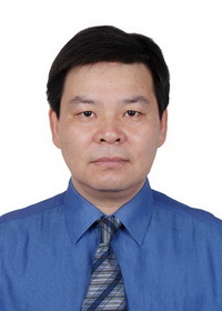 Chinhua Wang (王钦华)合作论文数School of Optoelectronic Science and Engineering, Soochow University;Key Lab of Modern Optical Techonologies of Education Ministry of China, Soochow University15
 Wenqiang Wan合作论文数13Jie Shao合作论文数University of Maryland, College Park, MD
13Jianfeng Xie (解剑峰)合作论文数Soochow University12
Wenqiang Wan合作论文数13Jie Shao合作论文数University of Maryland, College Park, MD
13Jianfeng Xie (解剑峰)合作论文数Soochow University12 Jianhong Wu (吴建宏)合作论文数School of Optoelectronic Science and Engineering, Soochow University11Fengbin Zhou合作论文数10Yimin Lou合作论文数9
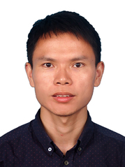 Zhenwu Shi (石震武)合作论文数School of Optoelectronic Science and Engineering, Soochow University9
 Yanyan Wang (王艳艳)合作论文数School of Optoelectronic Science and Engineering, Soochow University9Zhou-Ying Jiang合作论文数8Shi-Qing Zhao合作论文数8Zhiwei Lu (陆志伟)合作论文数Soochow University8Jin Hu (胡进)合作论文数8
 Yishen Xu (许宜申)合作论文数School of Optoelectronic Science and Engineering, Soochow University8Yan Shen (沈雁)合作论文数SVG Optronics Co., Ltd7WU Zhi-hua合作论文数6
 Dong Xiaoxuan合作论文数6ZhenHua Wang (汪振华)合作论文数6Zhang, F.合作论文数6
 Jianlong Xu (徐建龙)合作论文数College of Nano Science & Technology, Soochow University6
 Tao Yue (岳涛)合作论文数School of Electronic Science and Engineering, Nanjing University6
 Tao Lv合作论文数School of Electronic Science and Engineering, Nanjing University5Renjin Shao合作论文数5Wang Yanyan合作论文数5Donghui Yi合作论文数5Jiacheng Shi合作论文数5Tianchi Yang合作论文数5Ming Zhu合作论文数5Bing Xu (徐兵)合作论文数5Dayun Huo合作论文数5
 Jianxin Tang (唐建新)合作论文数Institute of Functional Nano & Soft Materials, Soochow University5
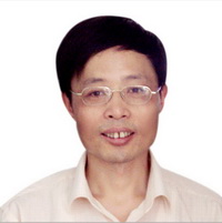 Weimin Shen (沈为民)合作论文数School of Optoelectronic Science and Engineering, Soochow University5




