Multimode cavity optomechanical systems allow light to couple otherwise non-interacting mechanical resonators, enabling non-Hermitian phenomena such as exceptional points, where eigenfrequencies and eigenvectors of coupled modes coalesce. Accessing an exceptional point and its nearby parameter space is a first step towards chiral mode dynamics and topological state transfer. Diamond optomechanical devices support strong coherent optomechanical coupling required to tune resonances to an exceptional point, as well as strain-coupling to spin-defects for hybrid quantum technologies, but have not yet been used for multimode non-Hermitian physics. Here we tune to an exceptional point in a diamond optomechanical crystal, which uses structural symmetry breaking to produce two high-frequency mechanical resonances coupled to an optical cavity. The exceptional point is reached within a stable operating window below the phonon-lasing threshold, and we observe asymmetric redistribution of optomechanical damping and anti-damping between hybridized modes. These results establish diamond optomechanical crystals as a platform for non-Hermitian optomechanics, opening routes to topological mechanical dynamics in hybrid spin-phonon interfaces.
Momentum-resolved electron energy loss spectroscopy (qEELS) in the low-loss (from 0 to ≈10 eV) region provides means for measurement of sample optical properties at the nanoscale. When both energy loss ΔE=ħω and momentum transfer q are measured, the dispersion relation of surface-plasmon polaritons (SPP) can be studied. However, the momentum (q) dispersion calibration is challenging due to the small scattering angles involved, and the consequent lack of suitable calibration samples and methods. Here, we discuss how by fitting the experimental data to a simplified SPP dispersion formula, the momentum dispersion can be calibrated and the dielectric constant ϵr of a thin surface layer measured. The dielectric constant measured by SPP fitting is robust to small sample tilts and stays within ±11% over a -6 ° to +13.3 ° sample tilt relative to the incident-beam direction. Methods such as electron diffraction and chemical mapping, can be applied to the same area as examined by qEELS, potentially providing insights in materials structure and composition with its optical properties.
Nucleosomes are proven to be the fundamental unit of chromosome structure. The stacking and folding of the nucleosome fibers within a chromosome is not fully understood. One of the reasons for the incomplete understanding of chromosome internal structure is that a nucleosome, about 11 nm in diameter, can not be resolved within the large chromatids (∼ 700 nm diameter) of a chromosome. In a transmission electron microscope (TEM), the large difference in size between the small diameter nucleosomes and a chromosome results in an extremely low contrast arising from individual nucleosomes. Consequently, the nucleosome fiber can not be detected within an intact chromosome. In this study, we compared two different methods in TEM, namely the hollow cone illumination (HCI) TEM and wavelet transform (WT) analysis on bright-field TEM (BFTEM) images, to analyze internal structure of chromosomes at length scales ranging from 10 to 30 nm. Isolated chromosomes were expanded and the orientation of the chromatin fibers was measured by HCI TEM and by WT applied to BFTEM. We demonstrated that the results obtained by the two methods are in an agreement.
In plasmonics, nonlocal effects arise when the material response to optical excitations is strongly dependent on the spatial correlations of the excitation. It is well known that a classical free electron gas system supports local Drude volume plasmon waves. Whereas a compressible quantum electron gas system sustains hydrodynamic volume plasmons with nonlocal dispersion isotropic across all high-symmetry directions. Here, distinct from Drude and Hydrodynamic plasmon waves, we present the first observation of crystalline nonlocal volume plasmon waves. We use transmission-based momentum-resolved electron energy loss spectroscopy to measure the volume plasmon dispersion of silicon along all the fundamental symmetry axes, up to high momentum values (q ∼ 0.7 reciprocal lattice units). We show that crystalline nonlocal plasmon waves have a prominent anisotropic dispersion with higher curvature along the light-mass (ΓK & ΓL) axes, compared to the heavy-mass (ΓX) axis. We unveil the origin of this phenomenon by experimentally extracting the anisotropic Fermi velocities of silicon. Our work highlights an exquisite nonlocality-induced anisotropy of volume plasmon waves, providing pathways for probing many-body quantum effects at extreme momenta.
We investigated the effect of nanoparticle (NP) image broadening and its contrast change dependence on a support matrix thickness in a transmission electron microscope (TEM). We measured the effect of NP size and atomic number on its image broadening. Based on the experimental TEM images we generated tomograms of NPs on four types of support matrix. The measured shape aspect ratio of the NPs in such tomograms depends on the geometry of the support matrix. For example, the aspect ratio of 6 nm NP placed on a thin film with windowframe support is 1.14, while the aspect ratio of 6 nm NP on a rod-shaped support with 910 nm diameter is 1.67 in a tomogram.
Ultrafast electron microscopy techniques allow for the structural dynamics of materials to be studied, and are typically achieved by modifying a commercial electron microscope to grant optical access to both the cathode and sample regions. To enhance the temporal resolution of these techniques, the electron bunch probe can be compressed by intense terahertz pulses confined in a tapered waveguide structure. The necessary modifications for optical access and waveguide integration may not be viable on all commercial systems, and has the potential to compromise the column. NanoMi is an open-source, modular electron microscopy platform that is highly amenable to customization, making it ideal for establishing ultrafast functionality in addition to exploring terahertz-electron interactions.
Journal Article NanoMi: Progress on an Open-source Electron Microscope Get access Makoto Schreiber, Makoto Schreiber NRC-NANO, Edmonton, Alberta, CanadaDepartment of Physics, University of Alberta, Edmonton, Alberta, Canada Search for other works by this author on: Oxford Academic Google Scholar Marek Malac, Marek Malac NRC-NANO, Edmonton, Alberta, CanadaDepartment of Physics, University of Alberta, Edmonton, Alberta, Canada Search for other works by this author on: Oxford Academic Google Scholar Mark Salomons, Mark Salomons NRC-NANO, Edmonton, Alberta, Canada Search for other works by this author on: Oxford Academic Google Scholar Darren Homeniuk, Darren Homeniuk NRC-NANO, Edmonton, Alberta, Canada Search for other works by this author on: Oxford Academic Google Scholar Sam Ruttiman, Sam Ruttiman NRC-NANO, Edmonton, Alberta, CanadaDepartment of Physics, University of Alberta, Edmonton, Alberta, Canada Search for other works by this author on: Oxford Academic Google Scholar Xuanhao Wang, Xuanhao Wang Department of Computing Science, University of Alberta, Edmonton, Alberta, Canada Search for other works by this author on: Oxford Academic Google Scholar Olivier Adkin-Kaya, Olivier Adkin-Kaya Department of Electrical and Computer Engineering, University of Alberta, Edmonton, Canada Search for other works by this author on: Oxford Academic Google Scholar Mohammad Kamal, Mohammad Kamal Department of Electrical and Computer Engineering, University of Alberta, Edmonton, Canada Search for other works by this author on: Oxford Academic Google Scholar Jesus Alejandro Marin Calzada, Jesus Alejandro Marin Calzada Department of Physics, University of Alberta, Edmonton, Alberta, Canada Search for other works by this author on: Oxford Academic Google Scholar Patrick Price, Patrick Price NRC-NANO, Edmonton, Alberta, Canada Search for other works by this author on: Oxford Academic Google Scholar ... Show more Martin Cloutier, Martin Cloutier NRC-NANO, Edmonton, Alberta, Canada Search for other works by this author on: Oxford Academic Google Scholar Misa Hayashida, Misa Hayashida NRC-NANO, Edmonton, Alberta, Canada Search for other works by this author on: Oxford Academic Google Scholar Ray Egerton, Ray Egerton Department of Physics, University of Alberta, Edmonton, Alberta, Canada Search for other works by this author on: Oxford Academic Google Scholar Ken Harada, Ken Harada Center for Emergent Matter Science, RIKEN, Hatoyama, Saitama, Japan Search for other works by this author on: Oxford Academic Google Scholar Yoshio Takahashi, Yoshio Takahashi Research & Development Group, Hitachi, Ltd., Hatoyama, Saitama, Japan Search for other works by this author on: Oxford Academic Google Scholar Heiko Müller Heiko Müller CEOS GmbH, Heidelberg, Germany Search for other works by this author on: Oxford Academic Google Scholar Microscopy and Microanalysis, Volume 29, Issue Supplement_1, 1 August 2023, Pages 489–490, https://doi.org/10.1093/micmic/ozad067.232 Published: 22 July 2023
We explore the properties of elastic and inelastic scattering in a thick organic specimen, together with the mechanisms that provide contrast in a transmission electron microscope (TEM) and scanning-transmission electron microscope (STEM). Experimental data recorded from amorphous carbon are used to predict the bright-field image intensity, mass-thickness contrast and dose-limited resolution as a function of thickness, objective-aperture size, and primary-electron energy E0. Combining this information with estimates of chromatic aberration, objective-aperture diffraction and beam broadening in the specimen, we calculate the achievable TEM and STEM resolution to be around 4 nm at E0 = 300 keV (or below 3 nm at MeV energies) for a 10 mu mdiameter objective aperture and 1 - 2 mu m thickness of hydrated biological tissue. The 3 MeV resolution for a 10 mu m tissue sample is probably closer to 10 nm. We also comment on the error involved in quadrature addition of resolution factors, when one or more of the point-spread functions are non-Gaussian.
Journal Article NanoMi: An Open Source Electron Microscope Component Integration Get access M Malac, M Malac NRC-NANO, Edmonton, CanadaDepartment of Physics, University of Alberta, Edmonton, Canada Search for other works by this author on: Oxford Academic Google Scholar D Homeniuk, D Homeniuk NRC-NANO, Edmonton, Canada Search for other works by this author on: Oxford Academic Google Scholar M Kamal, M Kamal Electrical Engineering, University of Alberta, Edmonton, Canada Search for other works by this author on: Oxford Academic Google Scholar J Kim, J Kim Electrical and Comp. Eng., University of British Columbia, Vancouver, Canada Search for other works by this author on: Oxford Academic Google Scholar M Salomons, M Salomons NRC-NANO, Edmonton, Canada Search for other works by this author on: Oxford Academic Google Scholar M Hayashida, M Hayashida NRC-NANO, Edmonton, Canada Search for other works by this author on: Oxford Academic Google Scholar J A Marin-Calzada, J A Marin-Calzada Department of Physics, University of Alberta, Edmonton, Canada Search for other works by this author on: Oxford Academic Google Scholar D Vick, D Vick NRC-NANO, Edmonton, Canada Search for other works by this author on: Oxford Academic Google Scholar D Price, D Price NRC-NANO, Edmonton, Canada Search for other works by this author on: Oxford Academic Google Scholar RF Egerton RF Egerton Department of Physics, University of Alberta, Edmonton, Canada Search for other works by this author on: Oxford Academic Google Scholar Microscopy and Microanalysis, Volume 28, Issue S1, 1 August 2022, Pages 3164–3165, https://doi.org/10.1017/S1431927622011746 Published: 01 August 2022
Germanium is typically used for solid-state electronics, fiber-optics, and infrared applications, due to its semiconducting behavior at optical and infrared wavelengths. In contrast, here we show that the germanium displays metallic nature and supports propagating surface plasmons in the deep ultraviolet (DUV) wavelengths, that is typically not possible to achieve with conventional plasmonic metals such as gold, silver, and aluminum. We measure the photonic band spectrum and distinguish the plasmonic excitation modes: bulk plasmons, surface plasmons, and Cherenkov radiation using a momentum-resolved electron energy loss spectroscopy. The observed spectrum is validated through the macroscopic electrodynamic electron energy loss theory and first-principles density functional theory calculations. In the DUV regime, intraband transitions of valence electrons dominate over the interband transitions, resulting in the observed highly dispersive surface plasmons. We further employ these surface plasmons in germanium to design a DUV radiation source based on the Smith-Purcell effect. Our work opens a new frontier of DUV plasmonics to enable the development of DUV devices such as metasurfaces, detectors, and light sources based on plasmonic germanium thin films.
The higher order structure of the metaphase chromosome has been an enigma for over a century and several different models have been presented based on results obtained by a variety of techniques. Some disagreements in the results between methods have possibly arisen from artifacts caused during sample preparation such as staining and dehydration. Therefore, we treated barley chromosomes with ionic liquid to minimize the effects of dehydration. We also observed chromosomes on a film with holes to keep pristine chromosome structure from being flattened as seen when placed on a continuous support film. A chromosome placed over a hole in a thin carbon film was mounted on a tomography holder, and its structure was observed in three dimensions (3D) using electron tomography. We found that there are periodic structures with 300-400 nm pitch along the axis in barley chromosomes. The pitch sizes are larger than those observed in human chromosomes.
In regions of adult neurogenesis, neural progenitor cells (NPCs) are found in close proximity to blood vessels within a so-called 'vascular niche'. Neurogenesis is linked to angiogenesis via certain growth factors. We propose that angiopoietin-1 (Ang1), which is similar to VEGF, has a unique role in neurogenesis independent of its role in angiogenesis. In this study, primary cultures of NPCs were transduced with recombinant adenoviruses expressing Ang1 and induced to differentiate with dibutyryl cyclic AMP (dbcAMP). Neuronal differentiation was evaluated by quantitative PCR, immunofluorescence microscopy and Western blot analysis. The results show that ectopic expression of Ang1 promotes neuronal differentiation and neurite outgrowth in NPCs, while this effect was blocked by the presence of anti-Tie2 receptor antibody or the PI3-K inhibitor, LY294002. Our results suggest that Ang1, identified originally as an angiogenic factor, can also stimulate in vitro neurogenesis in NPCs through the Akt pathway.
Journal Article In-situ Calibration for Angle-resolved Valence EELS Get access M Malac, M Malac NRC-NANO, Edmonton, CanadaDepartment of Physics, University of Alberta, Edmonton, Canada Search for other works by this author on: Oxford Academic Google Scholar M Hayashida, M Hayashida NRC-NANO, Edmonton, Canada Search for other works by this author on: Oxford Academic Google Scholar H Müller, H Müller CEOS GmbH, Englerstr. 28, D-69126 Heidelberg, Germany Search for other works by this author on: Oxford Academic Google Scholar Y Taniguchi, Y Taniguchi Hitachi High-Tech Corp., Hitachinaka-shi, 882 Ichige, Ibaraki-ken, Japan Search for other works by this author on: Oxford Academic Google Scholar RF Egerton RF Egerton Department of Physics, University of Alberta, Edmonton, Canada Search for other works by this author on: Oxford Academic Google Scholar Microscopy and Microanalysis, Volume 28, Issue S1, 1 August 2022, Pages 2032–2034, https://doi.org/10.1017/S1431927622007887 Published: 01 August 2022
Energy-filtering transmission electron microscopy (TEM) and bright-field TEM can be used to extract local sample thickness $t$ and to generate two-dimensional sample thickness maps. Electron tomography can be used to accurately verify the local $t$ . The relations of log-ratio of zero-loss filtered energy-filtering TEM beam intensity ( $I_{{\rm ZLP}}$ ) and unfiltered beam intensity ( $I_{\rm u}$ ) versus sample thickness $t$ were measured for five values of collection angle in a microscope equipped with an energy filter. Furthermore, log-ratio of the incident (primary) beam intensity ( $I_{\rm p}$ ) and the transmitted beam $I_{{\rm tr}}$ versus $t$ in bright-field TEM was measured utilizing a camera before the energy filter. The measurements were performed on a multilayer sample containing eight materials and thickness $t$ up to 800 nm. Local thickness $t$ was verified by electron tomography. The following results are reported: • The maximum thickness $t_{{\rm max}}$ yielding a linear relation of log-ratio, $\ln ( {I_{\rm u}}/{I_{{\rm ZLP}}})$ and $\ln ( {I_{\rm p}}/{I_{{\rm tr}}} )$ , versus $t$ . • Inelastic mean free path ( $\lambda _{{\rm in}}$ ) for five values of collection angle. • Total mean free path ( $\lambda _{{\rm total}}$ ) of electrons excluded by an angle-limiting aperture. • $\lambda _{{\rm in}}$ and $\lambda _{{\rm total}}$ are evaluated for the eight materials with atomic number from $\approx$ 10 to 79. The results can be utilized as a guide for upper limit of $t$ evaluation in energy-filtering TEM and bright-field TEM and for optimizing electron tomography experiments.
Bright-field transmission electron microscope (BFTEM) images exhibit spurious image intensity in the vacuum near the sample edge. The spurious intensity gradually decreases with increasing distance from the sample edge. By taking into account angular and energy loss distribution of the scattered electrons and lens aberrations, the origin of the spurious intensity of BFTEM images can be explained. The spurious intensity extent and magnitude can be significantly reduced by using either electron energy filtering or a small collection semiangle.
Electron tomography (ET) has been used for quantitative measurement of shape and size of objects in three dimensions (3D) for many years. However, systematic investigation of repeatability and reproducibility of ET has not been evaluated in detail. To assess the reproducibility and repeatability of a protocol for measuring size and three-dimensional (3D) shape parameters for nanoparticles (NPs) by ET, an inter-laboratory comparison (ILC) has been performed. The ILC included six laboratories and six instruments models from three instrument manufacturers following a standard measurement protocol. A technical specification describing the normative steps of the protocol is published by the International Standards Organization (ISO). Gold NPs with 30 nm nominal diameter contained within a rod-shaped carbon support were measured. The use of a rod-shaped sample support eliminated the missing wedge effect in the experimental tilt series of projected images for improved quantification. A total of 443 NPs were initially measured by NRC-NANO and then 115 out of the 443 NPs were measured by five other labs to compare measurands such as the Volume (V), maximum Feret diameter (Fmax), minimum Feret diameter (Fmin), volume-equivalent diameter (Deq) and aspect ratio (Frat) of the NPs. The results of the five labs were compared with the results obtained at NRC-NANO. The maximum disagreement in measurements of Fmin and Fmax obtained by the participating labs did not exceed 7 %. The measured Deq was between 27.5 nm and 30.3 nm in agreement with the NP manufacturer's specification (28 nm-32 nm). In addition to the above, the influence of the missing wedge effect and beam-induced NP movement was quantified based on the differences of the results between labs.
An abstract is not available for this content so a preview has been provided. As you have access to this content, a full PDF is available via the ‘Save PDF’ action button.
We provide an update on a public-license electron microscope (EM) platform [1], referred to as NanoMi. The optics are modular, allowing assembly of a TEM, scanning TEM (STEM) or an SEM (discussed here) within an independent vacuum envelope. Weakly Reciprocal
In this paper, we review the current state of phase plate imaging in a transmission electron microscope. We focus especially on the hole-free phase plate design, also referred to as the Volta phase plate. We discuss the implementation, operating principles and applications of phase plate imaging. We provide an imaging theory that accounts for inelastic scattering in both the sample and in the hole-free phase plate.
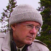 Ray Egerton合作论文数Department of Physics, University of Alberta;Department of Physics, Portland State University;National Institute of Nanotechnology79
 Misa Hayashida合作论文数44
 Marco Beleggia合作论文数Center for Functional Nanomaterials, Brookhaven National Laboratory23
 Yimei Zhu合作论文数Center for Functional Nanomaterials, Brookhaven National Laboratory;Institute for Advanced Electron Microscopy, Brookhaven National Laboratory21
 Robert A. McLeod合作论文数Hitachi High-tech Canada Inc.16
 Feng Wang合作论文数Brookhaven National Laboratory, Brookhaven National Laboratory15Masahiro Kawasaki合作论文数Inst Cosm Ray Res, Univ Tokyo14
 Peng Li合作论文数14
 Alkiviathes Meldrum合作论文数Faculty of Science, University of Alberta/Grayflare Inc.14
 Darren Homeniuk合作论文数11
 Hui Qian合作论文数National Institute for Nanotechnology11
 Mario Sergio Moreno合作论文数Organic Chemistry Department, Cordoba University10Ken Harada合作论文数9
 Mark R. Freeman合作论文数Department of Condensed Matter Physics, University of Alberta9
 Mark Salomons合作论文数8Yoshifumi Taniguchi合作论文数8Simon Hettler合作论文数Laboratory for Electron Microscopy, Karlsruhe Institute of Technology, Engesserstrasse 7, Karlsruhe 76131, Germany7Li Peng合作论文数7
 Zubin Jacob合作论文数Elmore Family School of Electrical and Computer Engineering, College of Engineering, Purdue University7Michael Bergen合作论文数6Kai Cui合作论文数6
 Martin Cloutier合作论文数6
 Quan Li (李泉)合作论文数Department of Physics, The Chinese University of Hong Kong6
 Prashant Shekhar合作论文数Dept. of Electr. & Comput. Eng., Univ. of Alberta;c;Dept. of Electr. & Comput. Eng., Univ. of Alberta5
 Robert Wolkow合作论文数Department of Physics, Faculty of Science, University of Alberta5
 Ross Lockwood合作论文数University of Alberta, University of Alberta5
 Juan Wang (王娟)合作论文数School of Civil Engineering, Beijing Jiaotong University5
 Jillian Buriak合作论文数Department of Chemistry, Faculty of Science, University of Alberta5Zhigang Liu合作论文数5
 F. Paraguay-Delgado合作论文数Centro de Investigación en Materiales Avanzados (CIMAV), Miguel de Cervantes 120, Complejo Industrial Chihuahua, Chih. 31109, Mexico5D. Hoyle合作论文数4Jesus Alejandro Marin Calzada合作论文数4Sean Chen合作论文数4Doug Vick合作论文数4emi kano合作论文数4
 Sayed Youssef Sayed合作论文数Chem Dept, Cairo Univ4p m price合作论文数4Konyuba Yuji合作论文数JEOL Ltd.4
 Michael Brett合作论文数Department of Electrical and Computer Engineering, University of Alberta4H Furukawa合作论文数4
 Ming-Wen Chu合作论文数Nanomaterials Laboratories, National Institute for Materials Science4
 Jason L Pitters合作论文数Department of Chemistry, McMaster University4
 June Lau合作论文数4
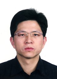 Huairuo Zhang合作论文数Institute of Physics Chinese Academy of Sciences, Chinese Academy of Sciences4Xuanhao Wang合作论文数3Isamu Ishikawa合作论文数3Olivier Adkin-Kaya合作论文数3Sohei Motoki合作论文数3




