Copper Zinc Tin Sulphide (CZTS) thin film solar cell achieved a great attention of researchers due to its optimum direct energy gap, higher absorption coefficient and good electronic properties. In this work, the CZTS/CdS based solar cell structure with and without back surface field (BSF) layer has been investigated numerically by using SCAPS-1D. Firstly, a basic experimentally reported structure (FTO/ZnO/CdS/CZTS/Mo) without BSF layer is considered and replicated. Then, by inserting p-CZTSe material as BSF layer in between the absorber and back contact, a new device structure (FTO/ZnO/CdS/CZTS/CZTSe/Mo) has been proposed. The performance of both structures; with and without BSF layer, have been analyzed with respect to different layer parameters like: thickness, carrier concentration, and defect densities (Nt). A negative effect on cell performance has been observed with working temperature. From these analyses the optimum conversion efficiency of CZTS based PV cell without BSF layer has been found to be around 8.55% using CZTS absorber. The cell with CZTSe BSF layer (FTO/ZnO/CdS/CZTS/CZTSe/Mo) gives an overall conversion efficiency of 22.03%. The efficiency of both cells improved by replacing back contact metal with higher work function. This study gives the highest efficiency of about 29.86% for FTO/ZnO/CdS/CZTS/CZTSe/Pt structure. These simulation results could be an important guideline to a researcher for fabricating cost effective, non-toxic, and highly efficient CZTS solar cells.
The effects of annealing and variation of temperature on the electrical and thermoelectric properties of e-beam evaporated InSe thin films has been investigated in details. The XRD study demonstrates that the as-deposited InSe thin films are amorphous while they become polycrystalline with the presence of In3Se4 phase after annealing. The SEM micrographs reveal that the surfaces of as-deposited films are smooth whereas they become non-uniform due to annealing. The heating and cooling cycles of the as-deposited films exhibit that the resistivity of the films shows an irreversible phase-transition and become stable after 3–4 successive heat-treatment operations in air. The electrical conductivity of annealed InSe thin films shows a highly degenerate semiconducting (metallic) behavior. The thermopower of the annealed films indicates that InSe thin film is a highly degenerate n-type semiconductor i.e. metallic. Thickness dependence thermopower obeys the Fuchs-Sondheimer theory. The optical band gap of the annealed films increases as compared to the as-deposited films. These results indicate that InSe thin films encounter a phase-transformation from In2Se3 to a new In3Se4 metallic phase with an optical band gap of ∼1.8 eV due to heat-treatment.
Nonradiative recombination (NRR) centers in GaAs:N δ-doped superlattices (SLs) grown by molecular beam epitaxy (MBE) has been investigated by two-wavelength excited photoluminescence (TWEPL) method for conduction band scheme. The PL intensity of E. band of the samples with lower nitrogen (N) concentration (0.317% N) initially increases after addition of below-gap excitation (BGE) light over above-gap excitation (AGE) light and then quenches at higher BGE density and energy, while that of GaAs (e-A°) emission of GaAs layers decreases monotonically. For sample with higher N concentration (1.18% N) both the E. band and GaAs (e-A°) emission decreases monotonically with enhancing BGE density and degree of decreasing of PL intensity is higher compared to the low N concentration sample. The quenching of PL intensity indicates the existence of NRR centers in GaAs layers and GaAs:N δ-doped SL region. The recombination models have been proposed for explaining the results from the experiments.
The V (5wt.%) doped In2O3 (V: In2O3) thin films with the thickness of 50–150nm were deposited on to glass substrate by electron beam evaporation technique and the deposited films were annealed at 200°C in air for 2h. The annealed films were characterized by structural, electrical, optical and photoluminescence properties. X-ray diffraction (XRD) pattern shows that the film is an amorphous nature. The negative sign of the Hall coefficient indicates the n-type conductivity. Experimental results show that the resistivity and transmittance of the films are strongly influenced by film thickness and post deposition annealing. A minimum resistivity of 6.22×10⁻³Ωcm, a carrier concentration of 5.23×1019cm−3, a Hall mobility of 19.21cm2V−1s−1 and a figure of merit of 1.04×10⁻⁴Ω−1 are observed for the film with thickness of 150nm. After annealing the films, the average transmittance is enhanced up to 84% in the near infrared region. The blue-shift of optical band gap is found to increase from 1.62 to 2.25eV with increasing the thickness, whereas the refractive index decreases from 2.92 to 2.64. Structural disorder was observed from the Urbach’s tail. A prominent and high intense orange emission is achieved at room temperature, which may be attributed to oxygen deficiencies or intrinsic defects.
Vanadium (5 at. %) doped Indium Oxide (V: In2O3) thin films with different thicknesses (50 nm, 100 nm and 150 nm) were prepared onto glass substrate by electron beam evaporation technique in a vacuum of about 4×10⁻³ Pa. X-ray diffraction (XRD) pattern revealed that the prepared films of thickness 50 nm are amorphous in nature. Temperature dependence of electrical resistivity was studied in the 300 < T < 475 K temperature range. The films exhibit a metallic behavior in the 300 < T < 380 K range with a positive temperature coefficient of the resistivity (TCR), whereas at T > 380 K, the conduction behavior turns into a semiconductor with a negative TCR. Optical studies revealed that the films of thickness 50 nm possess high transmittance of about 86 % in the near-infrared spectral region. The direct optical band gap lies between 3.26 and 3.00 eV depending on the film thickness.
Two-wavelength excited photoluminescence, a non-destructive and non-contacting method for defect study has been used to investigate the AlGaN multiple quantum well (MQW) emitting at ~260 nm. We have succeeded to detect the non-radiative recombination (NRR) centers in both wells and barrier layers using a below-gap ex- citation (BGE) light of 1.17 eV. The PL intensity of both well and barrier layers decreases after irradiation of BGE which can be explained by the well-established two-level model. The normalized PL intensity decreases with increasing BGE power density for both cases but more pronounced for the barrier layer. The normalized PL intensity increases for both well and barrier layer's emission with increasing AGE density and becomes saturated at higher excitation due to the fill-up of NRR centers.
CIS (Cu-InSe) thin films were prepared onto glass substrate by the two stage process—generally called bilayer process. At first, Cu layer was deposited onto glass substrate by electron beam evaporation technique and then InSe single layer was deposited on the resulting Cu layer to produce CIS thin film. XRD (X-ray diffraction) analysis revealed that deposited film has an amorphous nature. Electrical resistivity measurements were carried out as a function of temperature during heating and cooling cycles in air. The heating and cooling cycles of the sample are almost reversible after successive heat-treatment in air. In order to consider the influence of the InSe upper layer on the optical properties, the thickness of the InSe upper layer in the CIS films was varied from 50 to 150 nm. Analysis of the transmittance and reflectance spectra, recorded in the wavelength range of 400-1,100 nm, revealed that the CIS films have high absorption coefficient of ~10 cm. The direct band gap varies from 1.40 to 1.22 eV. The refractive index, the extinction coefficient and the dielectric constant of the CIS films depend on the film thickness.
Impregnation of pores of porous silicon (PS) by Lanthanum Fluoride (LaF3) using a novel one-step chemical bath technique, and application of the LaF3-impregnated porous silicon (PS) structure (LaF3/PS) as a potentiometric fluoride ion sensor have been investigated in this article. The impregnation of LaF3 inside the pores of porous silicon was achieved using a chemical bath technique developed by this group. The Scanning Electron Microscopy (SEM) and EDX on the cross-section of LaF3/PS/Si structure confirmed the LaF3 film deposition inside the pores of PS. The heterostructure of LaF3/PS/Si was investigated as fluoride ion (F - ) sensor in aqueous medium. The high specific area of PS was taken as the key subject to investigate the high fluoride sensitivity of the LaF3/PS structure in aqueous medium. When experimented with home made fluoride solution having various concentrations the annealed LaF3/PS/Si structure was found to detect the fluoride ion in aqueous solution. Its response was found linear in the fluoride concentration range of 2.28~4.28 pF. As capacitive sensor the overall fluoride sensitivity was found to be over-Nernstian (400 mV/pF). The experimental results indicate that LaF3-impregnated porous silicon structure (LaF3/PS) can be used as a high-sensitive fluoride-ion sensor in aqueous medium.
Chromium Oxide (Cr2O3) thin films have been prepared by thermal evaporation onto glass substrate at a pressure of about 6x10(-4) Pa. Structural and compositional analysis has been carried out by XRD, SEM and EDAX method. The heating and cooling cycles of the samples are reversible in the investigated temperature range after successive heat-treatment in air. Temperature dependence of electrical conductivity shows a semiconducting behavior. The thickness dependence of conductivity is well in conformity with the Fuchs-Sondheimar theory. The Hall coefficient shows a positive sign exhibiting p-type carriers. Optical study has been employed to determine the band gap of the samples.
 Jaker Hossain合作论文数Department of Applied Physics and Electronic Engineering, University of Rajshahi6
 K. A. Khan合作论文数Faculty of Sciences;University of Nis;Faculty of Sciences, University of Nis6
 Ratan Chandra Roy合作论文数4
 Md. Ariful Islam合作论文数4
 Norihiko Kamata合作论文数2
 M. A. Newaz合作论文数1
 Md Sohel Rana合作论文数1
 Md Mazharul Islam合作论文数1
 Md. Dulal Haque合作论文数1Md. Earul Islam合作论文数1
 Md Jakir Hossain合作论文数1
 Jannatul Robaiat Mou合作论文数Dept Elect & Telecommun Engn, Rajshahi Univ Engn & Technol1
 B.K. Mondal合作论文数Solar Energy Laboratory, University of Rajshahi1
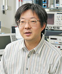 Hideki Hirayama (平山秀樹)合作论文数Terahertz Quantum Device Laboratory, RIKEN Center for Advanced Photonics1Shuhei Yagi合作论文数1
 Md. Hafijur Rahman合作论文数1
 Hiroyuki Yaguchi合作论文数1
 Yoshitaka Okada合作论文数Institute of Applied Physics, University of Tsukuba1Takeshi Fukuda合作论文数1
 A. Z. M. Touhidul Islam合作论文数1
 Abu Bakar Md. Ismail合作论文数1




