We report new measurements of the regrowth behaviour of Pb-implanted SrTiO3 crystals in the presence of water vapour. Doubly labelled water vapour, D218O, at greater than 95% enrichment in each isotope has been added to the annealing ambient and depth profiles of D and 18O have been obtained from the regrown crystals using secondary ion mass spectrometry (SIMS). The D and 18O content has also been measured by nuclear reaction analysis (NRA) using the reactions D(3He,p)4 He and 18O(p,6h)15 N. The crystals were regrown in a conventional furnace under a controlled gas ambient and time-resolved optical reflectivity (TRR) was used to dynamically monitor the regrowth rate during the anneal. An enhancement of the solid-phase epitaxial regrowth rate is observed when water vapour is added to the annealing ambient. This rate increase is accompanied by incorporation of D throughout the regrown layer. 18O is incorporated into the lattice but does not appear to penetrate deep enough to influence the regrowth rate.
Properties of ultrathin (~ 10nm) silicon nitride films on single crystal Si, InP and GaAs have been studied using Raman spectroscopy, medium energy ion scattering (MEIS), variable-energy positron annihilation spectroscopy and x-ray photoelectron spectroscopy (XPS). The silicon nitride films were prepared by remote microwave plasma chemical vapour deposition (RPCVD). The results showed that oxidation of the film due to air exposure was restricted to the near surface with an oxygen penetration depth no greater than 2 nm. The residual stress in the as-grown films was substrate-dependent. For films on Si(100), the film induced residual stress was compressive with a value of 0.5GPa. Annealing at 500°C for 60 minutes resulted in a complete release of the residual stress. Vacuum annealing at a temperature below 500°C also led to changes of the electrical properties in the films but not the substrate.
Copper is a prevalent contaminant in silicon device fabrication. Since Cu has high solubility in Sn, we are exploring the use of Sn to form Cu-Sn surface alloys as a means to inhibit Cu diffusion into Si substrates. Cu/Sn/Si (111) samples were prepared by MBE at 100°C, then annealed at temperatures between 300°C and 600°C. Resultant surface structures were imaged by AFM and SEM. AES and EDX were used to investigate the composition of two differently shaped clusters that formed after annealing. Etching with dilute HCI solutions was used to seek the chemical origin of various surface morphologies. The results are compared with those from Sn/Si and Cu/Si samples. A possible model for the evolution of 3-D structures in the Cu/Sn/Si(111) system will be presented.
Few non-destructive techniques are available which provide information regarding defect type, concentration and depth distribution in semiconductors. The variable-energy positron beam technique has recently demonstrated a sensitivity to near surface defects and impurities at low defect concentrations. In the present study, intrinsic silicon (100) epilayers of ~3000 Å thickness grown by MBE at different temperatures were examined by this method for evidence of changing defect concentration and type.
Significant progress has been realized in the use of quantum well intermixing (QWI) as a method for tailoring the bandgap energies of optoelectronic devices. Intermixing can be driven by an ion implantation process, an approach that appeals because of its simplicity, its planarity and its adaptability to selective area processing. Despite its success, the advantages of irradiation induced QWI need to be tested further and we report here current results of three research activities which address a) the existence or not of a simple scaling relationship which connects intermixing in a given QW structure for any ion species; b) reproducibility of intermixing in identical QW structures which have been obtained from different growth systems; and c) intermixing for above the well versus through the well implantation. A GaAs/AlGaAs MQW structure has been intermixed through ion irradiation followed by RTA annealing for 30s at 900°C. H, He and As ion species have been used with energies and fluences chosen so that similar defect profiles are generated by each ion species. Photoluminescence measurements at 12K reveal the bandgap energy changes in the irradiated QWs. Normalized for common concentrations of radiation induced defects, results show that intermixing increases with the mass of the incoming ion. Repeat measurements were undertaken using a set of four similar GaAs/AIGaAs structures, grown at three different laboratories by either metal organic vapour deposition or molecular beam epitaxy. The four structures show comparable QW energy shifts following implantation and RTA, indicating that variations in growth methods and techniques can be controlled so as not to unduly influence intermixing of the GaAs/AlGaAs heterostructure. Cross sectional scanning tunneling microscopy (XSTM) is used to examine the interdiffusion of a 20 period InGaAs/GaAs QW stack following P implantation and RTA. Implant energies are chosen so that the implanted ions either stop before reaching the QW stack or pass completely through it. For both cases, equal broadening is observed in the top and bottom QWs of the stack, suggesting that the defect flux is not attenuated as it passes though the QW region. When no defects are created at the depths of the QWs, enhanced group V, compared to group III, interdiffusion appears to occur at the well/barrier interfaces. Energy dispersive X-ray spectroscopy measurements are consistent with this observation. In contrast, no evidence is observed for preferential interdiffusion if the ions are implanted through a less heavily doped QW array.
We have examined the damage produced by Si-ion implantation into strained Si1-xGex epilayers. Damage accumulation in the implanted layers was monitored in situ by time-resolved reflectivity and measured by ion channelling techniques to determine the amorphization threshold in strained Si1-xGex, (x = 0.16 and 0.29) over the temperature range 30-110°C. The results are compared with previously reported measurements on unstrained Si1-xGex, and with the simple model used to describe those results. We report here data which lend support to this model and which indicate that pre-existing strain does not enhance damage accumulation in the alloy layer.
The reactivity of high-Fe containing sphalerite (Zn1−xFexS), the major source of Zn, is of great interest for industrial applications. Since the initial reactivity depends on the physical and chemical properties of the surface, it is important to understand the structure of cleaved and fractured surfaces. Zn1−xFexS zincblende (110) oriented samples cleaved in air and in vacuum were studied with medium energy ion scattering (MEIS) in order to study surface relaxation and reconstruction associated with the possible formation of S dimers. The experimental results are presented together with ion scattering Monte Carlo simulations that have been performed using the different models of the surface structure. The MEIS blocking patterns are different for the air- and vacuum-cleaved specimens. Models for the air-cleaved samples found S atoms in the first layer that are relaxed outwards by 0.08Å and Zn(Fe) atoms relaxed inwards by 0.51Å, with some lateral translation of both species. Results for the vacuum-cleaved sample indicate S atoms have been displaced laterally by 0.5Å at the surface. X-ray photoelectron spectroscopic (XPS) measurements provide evidence for a high binding energy species indicative of S–S bonds in the near-surface region that are consistent with the ion scattering structural data for both cleaving protocols.
Medium energy ion scattering has been used to study the kinetics of solid-phase epitaxial regrowth (SPEG) of ultrathin amorphous layers formed by room-temperature implantation of 5keV energy phosphorus ions into Si (100). The implants create P distributions with peak concentrations up to ∼7×1021cm−3. SPEG has been driven by rapid thermal annealing, 475°C⩽TA⩽600°C, for times up to 2000s. At each temperature, the regrowth velocity is enhanced in the early stages due to the presence of phosphorus but then slows sharply to a value more than an order of magnitude below the intrinsic rate. The critical phosphorus concentration at the transition point for TA=475°C regrowth is ∼6×1020cm−3 and increases steadily with anneal temperature. Time-of-flight secondary ion mass spectroscopy profiles confirm the onset of phosphorus push out, where the advancing recrystallization front enters the transition region. Supplementary cross-sectional transmission electron microscopy evidence confirms the existence of a local strain field.
We have implanted He3 into Si(100) at 1.0MeV ion energy and to fluences ranging between 2×10¹⁵ and 2×1016cm−2, followed by annealing at 700°C. Heating ramp rates have been systematically varied over more than two decades (0.3°C∕sto100°C∕s) at each fluence. The retention of He3 is measured through the He3(d,p)He4 nuclear reaction yield. We show that gas retention can be varied by more than an order of magnitude even while the other anneal parameters—anneal temperature and anneal time—are maintained constant. Cross-sectional scanning electron micrographs confirm the presence of planetarylike cavity structures at a depth closely matching that calculated for the damage peak.
Near-field diffraction element assisted lithography or DEAL has been used to fabricate two-dimensional lattice patterns in a photoresist. Specifically, a diffraction element was used to prepattern the coherent output of a laser prior to its capture in a photoresist. The pattern symmetry and spacing can be readily modified with the same experimental arrangement since the near-field diffraction pattern strongly depends on the nature of the diffractive element and the distance between the element and the photoresist. The patterns that are formed can serve as masks for patterning high index materials to create photonic band gap crystals. Alternatively, they have the potential to behave as two-dimensional photonic band gap arrays provided the polymer used exhibits a large enough index contrast.
Medium energy ion scattering (MEIS) has been used to study the kinetics of solid phase epitaxial regrowth (SPEG) of ultrathin amorphous layers created by room temperature implantation of 5keV energy phosphorus ions into Si(100). P ion fluences ranged from 5e14cm−2 up to 1e16cm−2, the associated a-Si thicknesses from 9.2nm to 20nm. Regrowth was driven by rapid thermal annealing for anneal temperatures 425°C⩽TA⩽600°C and for times up to 2500s. The Si(P) regrowth velocities exceed that of the intrinsic Si SPEG rate by an order of magnitude. Regrowth in the near surface is approximately 1.7 times slower than in the bulk. In Si implanted to high P fluence, Φ⩾5e15cm−2, regrowth is severely retarded when the recrystallization front intercepts P concentrations in excess of ∼1e21cm−3.
Si(100) wafers were implanted with 5-keV phosphorous (fluences of 1×10¹⁴–1×1016cm−2) and then annealed at 600–1000 °C, for 30 s or for 5 mins, to study shallow junction formation. Carrier densities were obtained by Van de Pauw Hall measurements, and carrier concentrations were depth profiled via a native-oxide stripping, differential Hall technique. For implanted fluences ⩾5×1014cm−2, an amorphous silicon surface layer is created. This results in solid-phase epitaxial growth at low annealing temperatures (600 °C), with reverse annealing upon dissolution of end-of-range interstitial clusters at higher temperatures (>700°C). Sheet resistances as low as 20Ω∕sq with electrical activation approaching 100% were achieved after annealing at 1000 °C.
A cavity stabilized, SESAM mode-locked Cr4+:YAG laser capable of generating sub-100 fs pulses has been developed. Locking the 130-MHz pulse repetition frequency to that of a hydrogen maser-referenced frequency synthesizer provides a 30-nm wide frequency comb for the 1530-nm wavelength region. In conjunction with a pair of acetylene stabilized, external cavity diode lasers, this laser provides a high precision measurement tool for the determination of acetylene transition frequencies.
Following a study of implantation enhanced interdiffusion of InGaAs∕InP multiple quantum well (MQW) structures by cross-sectional scanning tunneling microscopy (XSTM), the techniques of low temperature photoluminescence spectroscopy, high-resolution x-ray diffraction (HRXRD), and grazing incidence x-ray analysis (GIXA) are used to independently investigate the suitability of a square well model for the interdiffused MQW profiles, and the observed dependence of strain development as a function of the implanted ion range relative to the MQW stacks. In agreement with previous XSTM findings, when ions are implanted through the MQWs, HRXRD measurements indicate equivalent extents of interdiffusion occurring on both sublattices, while GIXA measurements further indicate the compositional profiles to be non-Fickian and compatible with uniformly broadened square well distributions. Following shallow ion implants (where ions are deposited between the MQWs and the sample surface), (004) HRXRD measurements indicate preferential group V interdiffusion. Dynamical simulations of the superlattice envelope in the (004) HRXRD rocking curves show the compositional profiles to be non-Fickian and compatible with a square well model for the broadened compositional profiles. Additional analysis of the (001) bilayer spacing from previously published XSTM linescan data for this structure is also consistent with this finding. Results of a preliminary photoluminescence and HRXRD investigation of disordering induced by indium implants and the effects of extended annealing on a series of MQW samples (with and without implantation) are presented. Implications for the implantation enhancement of interdiffusion in the InGaAs∕InP material system are discussed. The interpretation of quantum well interdiffusion experiments in this material system in terms of Fickian diffusion models warrants revision in light of the present findings.
Phosphorous diffusion in silicon has been investigated for room-temperature implants of low energy (5, 10, and 30 keV) and fluence between 1×10¹⁴ and 5×1015cm−2, followed by rapid thermal annealing in the temperature range of 600–1000 °C. Depth profiles were extracted by time-of-flight secondary-ion-mass spectroscopy. For 5-keV energy implants below 1×1015cm−2 fluence, phosphorus preferentially diffused outwards, i.e., toward the sample surface. Nuclear reaction analysis in combination with chemical stripping of the oxide shows that as much as 50% of the P in annealed samples can accumulate at the surface oxide during a 30-s anneal. At all implant energies, indiffusion of P dominates in the regimes of higher fluence, higher anneal temperature, and longer anneal times.
Concentration profiles of ultra-shallow phosphorus implants in silicon have been extracted through use of time-of-flight SIMS in combination with nuclear reaction analysis. The phosphorus implants spanned the energy range 1–30 keV with fluences from 1e13 to 1e15 cm−2. The resonance in the nuclear reaction 31P(α,p0)34S at incident alpha particle energy 4.96 MeV was used to measure the total retained phosphorus for an implant fluence of 1e15 cm−2, hence quantifying the associated SIMS profile. For lower fluence implants, absolute profiles were recovered from the SIMS data by scaling the profile integrals. Over the implant energy and fluence ranges we have used we find no evidence for loss of phosphorus due to self-sputtering.
We have initiated a study to extract concentration profiles of ultra shallow phosphorous implants in silicon complementing published work on ultra shallow boron implant profiles. There is an ever-increasing interest in the production of p-n junctions in silicon to create the new generations of ultra large scale integrated (ULSI) devices. Such junctions can be formed by implantation do pants (such as B, P, and As) at lowered energies. Development of design tools and process implementation both require that accurate methods be available for confirming absolute do pant profiles. Traditionally, profiles have been extracted through the use of secondary ion mass spectroscopy (SIMS), Rutherford backscattering spectroscopy (RBS), nuclear reaction analysis (NRA) and electrical measurements such as spreading resistance profilometry. Results of ion implanted species can be checked by SIMS (J.G.M. van Berkum, et al Vac. Sci. Technol. B16 (1998) 298). However, the analysis of ultra shallow implants by standard SIMS techniques is not straightforward and is weak in quantitative measurements. There are several reasons for this. First, standard methods of SIMS are hampered by limits on the instrumental sensitivity, which may not be adequate to examine very low-dose implants. Second, the accuracy in quantifying standard SIMS at very shallow depth is limited, due to an initial transitional region within which the sample composition equilibrates with the primary ion beam. This initial equilibration is characteristic of the SIMS technique, and is highly reproducible. Considerable effort has been expended in understanding the details of the equilibrium process, nevertheless, it is complicated even in the simplest of situations and continues to present problems for accurate quantification. Third, in specific situations high mass resolution required to separate the species of interest, or its proxy, from other mass groups, including impurity groups. Although there has been many investigations to extract quantitative profiles by SIMS using relative sensitivity factors (RSF), they can be reproduced 20-30% under more controlled conditions (R.G. Wilson, S.W. Novak, J. Appl. Phys. 69 (1991) 466). However, there is a need for other methods to normalize SIMS results. RBS is a candidate to calibrate SIMS profiles, but lacks the sensitivity to detect phosphorous due to the proximity of its mass with the masses of Si isotopes. Nuclear reaction analysis (NRA), 31P( a ,p)34S, is a suitable method for phosphorous detection. This nuclear reaction displays a resonance in the cross section at an incident energy near 5 MeV. While the cross section for the 31P( a ,p)34S reaction is small, we are able to measure the absolute do pant concentration of phosphorous implants into Si down to fluences of 1 ´ 1014cm-2. This opens a route to the calibration of TOF SIMS integrated profiles for P, which may then be used for analysis of the lower fluence regime. Two sets of phosphorous implanted silicon wafers were prepared. Phosphorous doses in our samples ranged from 1 ´ 1013 cm-2 to 5 ´ 1015 cm-2 with the implanted energy of 1 keV to 30 keV. To date, no evidence was found for self-sputtering based on these samples. The alpha capture reaction on phosphorous has been investigated in the field of nuclear physics to find the nuclear energy level of different isotopes. This reaction has been used in profiling P in silicon, but none to P concentrations and P implanted energies as low as those reported here. The present studies complement the work done on ultra shallow boron implant (Aditya Agarwal, et al Appl. Phys. Lett. 74 (1999) 2453).
The medium energy ion scattering (MEIS) system at the University of Western Ontario has been modified by replacing the original one-dimensional position sensitive detector with a 2-D array. Calibration and analysis procedures for quantitative depth profiling are devised and established in this work: distortion correction, image tiling, charge state distribution of the scattered hydrogen ions, etc. The software to simultaneously control the sample manipulator (three orthogonal rotations), toroidal electrostatic analyzer and spectrum acquisition has been developed using LabViewR. This development makes for easy sample alignment to the incident ion beam and automatically collects the step images. Additionally, the tiling procedure using corrected step images is accomplished within LabViewR to produce a final energy–angle spectra. Our QUARK (quantitative analysis of Rutherford kinematics) spectrum simulation package has been modified to provide for non-linear least squares fitting to a measured MEIS energy spectrum. As a reference for quantitative analysis, a shallow Sb-implanted graphite sample was used with normalization to the height of the thick target carbon region by applying 1H stopping power values from Konac et al. [Nucl. Instr. Meth. Phys. Res. B 136–138 (1998) 159]. To determine the system suitability for compositional analysis, Zr silicate films of thickness 2–7 nm on Si (100) substrates have been characterized by MEIS, RBS and NRA. The absolute areal densities of constituent elements are in good agreement (within 15%) among the three methods.
A self-assembled array of nanometer-sized holes in alumina has been adapted as a mask for conventional, broad-area, ion implantation. The mask pattern, made up of nanoholes arranged in a two-dimensional triangular array with a 100 nm period and a 55 nm diameter pore size, has been successfully transferred onto single crystal (100) SrTiO3 substrates using 200 and 500 keV energy Pt ion bombardments, at fluences sufficient to amorphize the exposed areas. The amorphized material was removed by selective chemical etching resulting in a periodic array of holes about 55 nm in diameter and 115 nm deep. This parallel, nonlithographic approach is adaptable to submicron depth, variable array geometry and scale, and to any material where a selective etch can be found for the irradiated volume. (C) 2002 American Institute of Physics.
Single-crystal indium phosphide wafer samples have been implanted through a stencil mask with single energy indium ions at 2, 5, and 8 MeV to fluences of 2, 2, and 3 x 10(14) cm(-2), respectively. Specimens were then etched in a concentrated solution of HF: HNO3 at room temperature. Selective etching of the implanted regions resulted in transfer of the mask pattern to the InP substrate. Etch rates were determined from step height profilometry measurements across the patterned surface. A wet chemical etch rate of 1.7 +/- 0.2 mum/min was observed for the ion implanted material, a rate three orders of magnitude higher than the 2 nm/min measured for unimplanted single crystal material. (C) 2001 The Electrochemical Society.
 R. D. Goldberg合作论文数41S. Charbonneau合作论文数34
 W.N Lennard合作论文数33Todd W. Simpson合作论文数32
 Philip Poole合作论文数National Research Council of Canada29
 Usman Akano合作论文数Department of Physics, University of Western Ontario20Geof C. Aers合作论文数19P. G. Piva合作论文数19Peter J Simpson合作论文数Department of Physics and Astronomy, University of Western Ontario17PJ SCHULTZ合作论文数17
 Maarten Vos合作论文数Research School of Physical Sciences and Engineering, Australian National University14M. Dion合作论文数13Emil S. Koteles合作论文数GTE Laboratories Incorporated13Margaret Buchanan合作论文数12GR MASSOUMI合作论文数12Yongqi Feng合作论文数11
 Jianjun He (何建军)合作论文数College of Optical Science and Engineering, Zhejiang University11Liji Huang合作论文数10P. F. A. Alkemade合作论文数10w m lau合作论文数9C.J. Miner合作论文数9Ht Tang合作论文数8Shepherd, F.R.合作论文数7
 Siegfried Janz合作论文数Advanced Photonics and Electronics Research Centre, National Research Council of Canada7
 Jeffrey McCallum合作论文数School of Physics, University of Melbourne7Jean Marc Baribeau合作论文数National Research Council Canada7
 Colin Wu合作论文数7
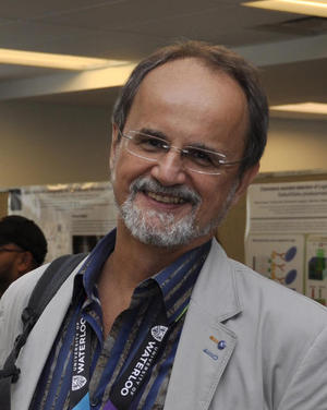 Zbigniew Wasilewski合作论文数Department of Physics and Astronomy, University of Waterloo7
 Joan E. Haysom合作论文数6T.E. Jackman合作论文数6S.Y. Tong合作论文数5Huajie Chen合作论文数5G.C. Weatherly合作论文数5
 Lynn A Boatner合作论文数Materials Science and Technology Division, Oak Ridge National Laboratory5Ruffell Simon合作论文数Research School of Physics and Engineering, Australian National University5R.L. Williams合作论文数5
 Randall M. Feenstra合作论文数Department of Physics, Mellon College of Science, Carnegie Mellon University/Department of Materials Science and Engineering, Carnegie Mellon University5
 Daniel Labrie合作论文数Department of Physics and Atmospheric Science, Dalhousie University5K. Griffiths合作论文数4
 David J. Lockwood合作论文数National Research Council of Canada4
 Simon Fafard合作论文数Departement de physique, Universite de Sherbrooke4
 Michael Nastasi合作论文数Department of Nuclear Engineering, College of Engineering, Texas A&M University4P. X. Zhang合作论文数4
 Paul McIntyre合作论文数McIntyre Laboratory, Department Materials Science and Engineering, Stanford School of Engineering, Stanford University;Precourt Institute for Energy, Stanford Doerr School of Sustainability, Stanford University4A. Dygo合作论文数4
 Peter Norton合作论文数Western University4John P. Mccaffrey合作论文数4H. Lafontaine合作论文数4n sylvain charbonneau合作论文数3




