Reports on news of interest to SPS society members.
The design of microwave circuits needs a good analysis of the performances of the field-effect transistor equivalent circuit. Indeed the small signal equivalent circuit of the field-effect transistors makes it possible to easily determine their performances such as the gain and the noise figure. A field-effect transistor constitutes a propagation structure along its gate width. Telegraphists’ equations are solved for this structure. One deduces from this the effect of the propagation on the transistor Z-parameters which can be taken into account in electric simulations and which may improve the use of long transistors at lower frequencies and of short transistors at higher frequencies.
This paper shows the VNA calibration for a DUT with a differential input and a single output embedded into a measurement board. Simulations have validated the concept.
Presents information on various MMTS Society chapters.
The well known TRL calibration method eliminates measurement errors at the input and output of a device under test (DUT). It uses a matrix formalism, which is not easy to realize in experimental software. In this article, we provide the analytical version of this calculation which may be easier to implement.
This paper shows the VNA calibration for a DUT with a differential input and a single output embedded into a measurement board. Simulations have validated the concept.
Founded in January, 2014 by Ph.D. students of the Integration from Material to Systems Laboratory, the BEE Branch is the IEEE Student Branch of Bordeaux. The BEE Branch aims at showing students in electronics engineering how they can benefit from the activities and membership in IEEE. For this sake, the BEE Branch organized three days of scientific interactions, featuring all of our students' chapters, lecturers, workshops and poster sessions that align with the actual stakes in Electronic Engineering.
Presents information on various MTTS Society chapters.
The variation of the linear inductance of a CPW with the frequency is used to extract the effective permeability that depends on the metallic losses. The result allows to separate the dielectric and metallic losses and to calculate some characteristics of the waveguide.
Semiconductor devices are tested within a complex environment including a loadboard and a socket. In this paper, we propose a calibration methodology and a RF de‐embedding technique that allows the extraction of the device parameters. This method is based on the utilization of several calibration elements inspired by the TRL method. This study has been applied on an active device and the results have been validated using a real test solution.
A bended and straight coplanar waveguides are modeled by using HFSS 3D electromagnetic software. The behavior of bend CPW is described by matrix calculations in order to show the effect of the parasitic even mode on the propagation of a signal. A comparison is done in this article with several works done before to show that there is a significant error when using bended CPW standard instead of straight ones in calibration.
The purpose of this article is to describe the effect of the parasitic even mode on the propagation of a signal along a bended coplanar waveguide and to evaluate the errors when bended standards are used in a TRL calibration instead of straight ones.
Presents information on MMTS Region 8 activities and events.
In this paper we present experimental characterization of packaged switch devices in terms of their RF attributes: isolation, insertion loss, power consumption, and linearity. Packaging and Board assembly significantly reduce their RF and mm-Wave performances. A broadband experimental setup is developed for the qualification of packaged switch devices accounting for deembedding effects both with on-board/on-package and on-chip probing. Module-based switch devices have been measured then, plastic molding, Si cap, and bonding wires have been sequentially removed to investigate their influences. Different challenges with packaged switch devices are identified and effective solutions are proposed for their qualification.
Presents information on the meeting of MTT-s chapter representatives in Paris, France.
Reports on major events and activities that were part of the MTT-S Mexico trip.
In this paper, modeling and experimental characterization of bond-wire arrays are proposed based on dedicated pilote carriers designed and fabricated for RF and microwave applications. Effects of the number of wire elements, connected in parallel to build bond-wire arrays, on the values of extracted broadband parasitics are investigated. Physical characterization of molding compound materials is proposed for their structural analysis and for broadband extraction of their dielctric properties (complex permittivity). Influence of molding compound properties on extracted parasitics of bond-wire arrays is highlighted.
Reports on recent trends and industry developments involving the MMTS society.
The work is related to an Agile Filter which is a specific RF block to be inserted between an antenna and a first stage of pre-amplification in future on board antenna systems or any future multi-purpose communications terminals. It will be able to process signals in the frequency range between 2 and 18 GHz with target insertion loss below 3dB. The basic idea of the demonstrator studied and developed in this project is to evaluate a SiP approach combining heterogeneous technologies and 3D integration and packaging. This paper presents the process flow used to design, fabricate and integrate in 3D a tunable RF filter which tunability is obtained by the use of MEMS varactors based on a copper on glass technology and stacked on micro-PCD for the electronic control functions. MEMS+ parameterized structures for RF MEMS varactor designs are presented with dimension constraints to be compatible with the space available at the end of each combline sub-filter. Indeed, the MEMS capacitors are composed of a mobile square membrane of 210μm by side and overall size of 600μm. In addition, these RF MEMS tunable capacitor models were automatically transferred into VerilogA for rapid system-level simulation usable further in ADS environment to verify the RF performances.
This paper presents a model for the crossover area of two crossing lines. The model was compared to 3D full wave electromagnetic simulation with good agreement up to 20 GHz.
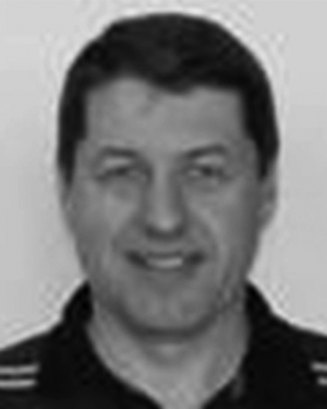 Philippe Descamps合作论文数18
 Jeanluc Gautier合作论文数17Pierre Pouvil合作论文数16
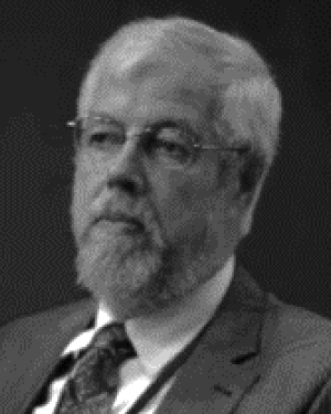 Jan Machac合作论文数Czech Technical University13
 Dominique Lesenechal合作论文数13Emmanuelle Bourdel合作论文数10sebastien quintanel合作论文数6
 Dr Kassem Hamze合作论文数ENSICAEN/CRISMAT/UMR6508, Normandie Université6
 Thanh Vinh Dinh合作论文数LaMIPS;c;LaMIPS6Boudiaf, A.合作论文数6Edouard De Ledinghen合作论文数5Antonio Bracale合作论文数5Ben Amor, M.合作论文数5
 Bruno Delacressonniere合作论文数5n fel合作论文数4
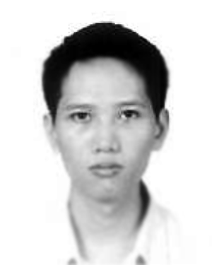 Linh Nguyen Tran合作论文数4Loulou, M.合作论文数4J.L. Pelloie合作论文数4Sébastien Quintanel合作论文数4
 Moez Balti合作论文数3Yiqun Li合作论文数3Descamps, P.合作论文数3
 Jean-Charles Bolomey合作论文数3V. Ferlet-Cavrois合作论文数3
 Benoit Derat合作论文数3
 Pierre Nicole合作论文数3
 Julien Pagazani合作论文数3
 Gaelle Lissorgues合作论文数3Jl Gautier合作论文数2f giannini合作论文数2bela szendrenyi合作论文数2JM WACRENIER合作论文数2Werling, T.合作论文数2
 frederique giannini合作论文数2Frederic Voiron合作论文数2Laurent Leyssenne合作论文数2Ben Salah, M.合作论文数2
 Sidina Wane合作论文数2Pierre Tabourier合作论文数2Christian Druon合作论文数2C. Dubon-Chevallier合作论文数2Christian Gautier合作论文数1C. Tolant合作论文数1S. Wane合作论文数1
 O. Tesson合作论文数1Michael Hoffmann合作论文数1Dubon-Chevalliewr, Chantal合作论文数1wojciech krzysztofik合作论文数1




