Raman-scattering spectroscopy has been used to study the folded longitudinal-acoustic (FLA) phonons in three- and four-layer superlattices comprised variously of slabs of GaAs, Ga 1-x Al x As, and AlAs. For each superlattice, the observed FLA peak frequencies recorded with different exciting wavelengths agree very well with the calculated dispersion relation based on an elastic-continuum model. However, apart from some qualitative trends in the three-layer superlattices, the relative intensities of the Raman FLA peaks are not well reproduced by the photoelastic theory of a perfect superlattice. Reasons for this discrepancy are discussed. The three-layer superlattices exhibited a high photoluminescence efficiency, comparable to that of strained Ga 1-x In x As/GaAs single quantum wells
Using transport measurements, we study resonant-tunneling transmission widths in a series of double-barrier samples grown by GaAs-based molecular-beam epitaxy. We find that the measured apparent resonance width is independent of the barrier and falls in the range of 1-5 meV. We propose two possible explanations: (a) a broadening of the observed width due to well-width variations (i.e., growth islands) across the device mesa or (b) a broadening limited by the electron-impurity scattering in the heavily doped contact regions. The latter has the important implication that the ultimate electron-energy resolution obtained from transport measurement is limited by the intrinsic width due to either inelastic- or even elastic-scattering processes in the reservoir.
The use of planar and axial channeling to measure the magnitude of the tetragonal distortion (and hence the strain) in simple strained-layer systems has been investigated. The test structures consisted of a 250 Å epitaxial InxGa1−xAs layer sandwiched between a (100) GaAs substrate and a thin (250–360 Å) surface GaAs epilayer. The In concentrations were sufficiently high (0.10–0.16) so that the resulting tilt or kink angle, Δ, at the buried interface exceeded the planar critical angle ψc for the 2.0 MeV4He+ beam. Complications in the observed axial and planar angular scans in the InGaAs layer have been studied in detail and suitable methods for extracting the correct values of Δ have been established. Planar channeling measurements, corrected for specular reflection effects in the GaAs surface layer, give Δ values in very good agreement with those calculated from the indium content. Axial channeling, however, can only be used to determine Δ when the surface GaAs overlayer is thinner than d/ψc, where d is the spacing between atomic strings.
Photoluminescence (PL) and laser emission from optically excited InxGa1−xAs–GaAs strained-layer superlattices (SLS) grown by molecular-beam epitaxy have been examined. In low-intensity PL, a single, narrow (≈5 nm FWHM) emission peak was observed, corresponding to the n = 1 electron to heavy-hole transition. This feature, as well as a series of higher energy transitions, was also observed in absorption and photoreflectance spectra. High-intensity PL, using a pulsed nitrogen laser for excitation, yielded an additional peak, several millielectronvolts lower in energy than the dominant low-power PL feature. Optical-gain measurements were performed using the variable stripe-length method. The stimulated emission emerging from the single cleaved end was shifted to the long-wavelength side of the low-power PL peak, and in the case of the narrower well samples, the emission consisted of two peaks separated by about 8 meV. Lasing at these gain positions was observed when ≈400 μm long chips were prepared and their lengths were pumped with a stripe of nitrogen laser light. The observed gain spectrum has been attributed to a combination of a free-carrier-induced bandgap shift and self-absorption by unpumped material deeper within the SLS waveguide.
The photoluminescence from the well region of a GaAs/AlGaAs double barrier resonant tunneling structure with a 5 nm thick well and 10 nm thick barriers is studied as a function of the applied voltage. The width, peak position and integrated area under the photoluminescence peak are all shown to be useful probes of the resonant current. Estimates of the built-in zero-bias potential, the electron density accumulated in the well and the characteristic tunneling time are inferred from the data and compared with theory.
The effect of excitation intensity on the photoluminescence spectra of pseudomorphic InGaAs/GaAs single quantum wells grown by molecular beam epitaxy is examined. Even at moderate excitation intensities, saturation of the exciton population and band-filling is observed. The band-filling leads to luminescence involving higher sub-bands, and the energies obtained are used to estimate the band offsets at the quantum well interfaces.
A nondestructive optical means of determining the activated hole concentration in p-type polar semiconductors is described. The Raman spectra from coupled plasmon-longitudinal-optical-phonon modes in five samples of Be-doped GaAs are measured and fitted using a theory which takes into account the degenerate light- and heavy-hole valence bands. The results indicate that coupled plasmon-longitudinal-optical-phonon modes in p-type material differ both quantitatively and qualitatively from those in n-type semiconductors.
We used non‐resonant, allowed Raman scattering to observe the coupled LO phonon‐plasmon modes in MBE‐grown p‐GaAs samples heavily doped with Be. With increasing hole concentration, the single coupled‐mode spectrum moves first from the unscreened LO phonon energy to higher energy, then shifts continuously back towards, and finally asymptotes at, the TO phonon energy. The Raman lineshapes at all densities are consistent with calculations when intervalence band, intra‐light hole and intra‐heavy hole band transitions are included in the system’s dielectric function.
Extrinsic luminescence due to carbon and beryllium acceptors in InGaAs pseudomorphic single quantum wells has been studied. The relative intensity is found to be very weak, even for acceptor concentrations ∼ 10 17 cm −3 . Acceptor binding energies are obtained and compared with those for GaAs/AlGaAs quantum wells and InGaAs/GaAs multilayer structures. Despite the relatively large strains in the InGaAs/GaAs single quantum wells, we do not observe any significant effect on the binding energies.
A photoluminescence (PL) study of InGaAs/GaAs strained quantum well (QW) structures is reported. Both fully strained and partially relaxed structures are examined, and the authors show that carrier localisation in the latter leads to enhanced extrinsic luminescence. Two other sources of localisation are considered, namely alloy and interface fluctuations, and their effect on the PL spectra is discussed. The effect of indium concentration (xIn) on the PL spectra is also examined, with greater surface roughening being observed at higher xIn, in turn leading to wider PL linewidths. Finally, they have examined the effect of nonradiative recombination in these QWS. In the unrelaxed layers the trap density is shown to be very low, while nonradiative recombination in the partially relaxed layers most likely occurs at electrically active extended dislocations.
The excitation of zone-folded longitudinal acoustic phonons in GaAs/InxGa1−xAs strained-layer superlattices is observed by Raman scattering. The Raman data agree well with theory and are consistent with high indium concentrations achieved in the fabrication of these metastable superlattices of good crystalline quality.
The growth of GaAs on Si(100) directly and with Ge buffer layers has been carried out sequentially under ultra high vacuum conditions in a double-ended III–V and group IV molecular beam epitaxy system. These heterostructures were examined by cross-section transverse emission microscopy, Rutherford backscattering, X-ray diffraction, and photoluminescence spectroscopy.Dislocation densities were observed to be high [Formula: see text] near both the GaAs–Si and the Ge–Si interfaces and to decrease to ~5 × 10 8 cm −2 a few micrometres from these interfaces. No dislocations were observed to originate at the GaAs–Ge interface, but the threading dislocations existing in the Ge buffer layer were found to propagate across this interface without significant deviation. The crystalline quality of the GaAs grown on Ge buffer layers was comparable with that grown on Si directly. However, GaAs has not yet been grown on the highest quality Ge buffer layers obtainable.
Results of Raman scattering experiments on (a) periodic superlattices made up of GaAs/InxGa1−xAs layers with high indium concentrations, (b) GaAs/Ga1−xAlxAs Fibonacci superlattices, are presented. We discuss the observed peak positions and intensities using the continuum theory of acoustic wave propagation in layered media and the photo-elastic coupling model.
Photoluminescence studies have been carried out on InGaAs pseudomorphic single quantum wells grown on GaAs by molecular beam epitaxy. Linewidths as narrow as 2.0 meV have been observed. The spectra typically consist of two peaks which on certain samples can be explained by intrawell thickness variations of one monolayer. On other samples the results are more consistent with exciton trapping at islands having a smaller lateral extent than the exciton Bohr radius.
A UHV MBE apparatus in which the deposition of both group IV and group III-V components is possible without breaking vacuum has been utilized to compare the growth of GaAs epilayers on non-polar Si(100) and Ge coated Si(100) substrates. In addition, a comparison of GaAs epilayers grown on substrates cleaned by ex-situ techniques and on substrates given all UHV in-situ surface preparation was made. Defect reduction by the incorporation of strained-layer superlattice dislocation filters and by post-growth rapid thermal anneal (RTA) thermal cycles was also investigated. Optical and material properties comparable to MBE grown GaAs/GaAs were obtained for GaAs grown on Ge coated Si(100) substrates.
 Wt Moore合作论文数10
 David J. Lockwood合作论文数National Research Council of Canada4
 Jeff F. Young合作论文数Department of Physics and Astronomy, The University of British Columbia3A. J. Springthorpe合作论文数3Peter B Mandeville合作论文数3MWC DHARMAWARDANA合作论文数2Margaret Buchanan合作论文数2
 Dolf Landheer合作论文数2Geof C. Aers合作论文数2T.E. Jackman合作论文数2Kam Wan合作论文数Colorado Research Associates Division, NorthWest Research Associates2BD ROUHANI合作论文数1n e j hunt合作论文数1r j stoner合作论文数1b m wood合作论文数1A. Rodriguez合作论文数1G. Aers合作论文数1H. Liu合作论文数1benjamin robinson合作论文数1Jie Zhao合作论文数1C.J. Miner合作论文数1
 D. A. Thompson合作论文数Department of Engineering Physics, McMaster University1J. Davies合作论文数1D. C. Houghton合作论文数1Jle Stevens合作论文数1
 B. K. Garside合作论文数Department of Engineering Physics, McMaster University1
 Leonard Dobrzynski合作论文数National Center for Scientific Research, Lille University1Jean Marc Baribeau合作论文数National Research Council Canada1P. Maigne合作论文数1J. Mendialdua合作论文数1Paul E Jessop合作论文数1John P. Mccaffrey合作论文数1H. Clive Liu合作论文数Impossible Foods1MW DENHOFF合作论文数1
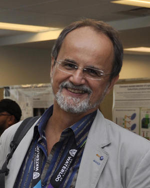 Zbigniew Wasilewski合作论文数Department of Physics and Astronomy, University of Waterloo1
 Allan MacDonald合作论文数Department of Physics, College of Natural Sciences, The University of Texas at Austin1




