Locating dopants in 3D is of great interest as advanced materials and devices increasingly rely on control at atomic dimensions, and microscopy tools are constantly in development for this purpose. One potential tool is electron energy loss spectroscopy (EELS) depth sectioning, where a core-loss signal is collected as a function of electron probe defocus along an atomic column in scanning transmission electron microscopy. Here we revisit its prospects through simulation with particular attention to dose considerations. We discuss pitfalls of by-inspection interpretation of EELS depth sectioning and resolve them by comparing with simulated references in a Bayesian framework. While direct electron detectors are starting to enable energy-filtered momentum-resolved maps, we show that momentum resolution offers no real advantage for depth determination. We extend the Bayesian framework to infer the depths of multiple dopants along a column without simulating all possible doping concentrations and configurations. We further show that zero-loss depth sectioning is too sensitive to residual aberrations to usefully allow the application of our Bayesian framework.
Surface structure affects the growth, shape and properties of nanoparticles. In wet chemical syntheses, metal additives and surfactants are used to modify surfaces and guide nanocrystal growth. To understand this process, it is critical to understand how the surface structure, and hence its energy, is modified. However, measuring the type and arrangement of atoms at hard-soft interfaces on nanoscale surfaces, especially in the presence of surfactants, is extremely challenging. Here, we determine the atomic structure of the hard-soft interface in a metallic nanoparticle by developing low-dose imaging conditions in four-dimensional scanning transmission electron microscopy that are preferentially sensitive to surface adatoms. By revealing experimentally the copper additives and bromide surfactant counterion at the surface of a gold nanocuboid and quantifying their interatomic distances, our direct, low-dose imaging method provides atomic-level understanding of chemically sophisticated nanomaterial surface structures. These measurements of the atomic structure of the hard-soft interface provide the information necessary to understand and quantify surface chemistries and energies and their pivotal role in nanocrystal growth. Surface controls nanocrystal growth, but atomic-scale hard-soft interfaces are hard to measure. Here, the authors develop electron microscopy methods to reveal the position of metal adatoms and surfactant counterions on gold nanocuboid surfaces.
Quantitative potential retrieval in scanning transmission electron microscopy (STEM) is of much importance for detailed material characterization but is often hindered by substantial multiple scattering effects in thicker samples. Here, we propose a gradient-descent-based optimization algorithm to obtain the quantitative potential from thick samples from a four-dimensional (4D) STEM dataset using the scattering matrix (S-matrix), which is an operator to calculate the exit-surface wavefunction in the presence of multiple scattering. This optimization uses optimum bright-field STEM data as an initial guess of potential and a loss function based on measured and estimated 4D STEM datasets without the regularization terms commonly used in iterative potential retrieval techniques in STEM. We show the capabilities of our approach through systematic simulations across a range of sample thicknesses, doses, and degrees of spatial incoherence and by applying it to experimental data. The extension of our algorithm from pixelated to segmented detectors is also investigated.
Surface structure affects the growth, shape and properties of nanoparticles. In wet chemical syntheses, metal additives and surfactants are used to modify surfaces and guide nanocrystal growth. To understand this process, it is critical to understand how the surface structure is modified. However, measuring the type and arrangement of atoms at hard-soft interfaces on nanoscale surfaces, especially in the presence of surfactants, is extremely challenging. Here, we determine the atomic structure of the hard-soft interface in a metallic nanoparticle by developing low-dose imaging conditions in four-dimensional scanning transmission electron microscopy that are preferentially sensitive to surface adatoms. By revealing experimentally the copper additives and bromide surfactant counterion at the surface of a gold nanocuboid and quantifying their interatomic distances, our direct, low-dose imaging method provides atomic-level understanding of chemically sophisticated nanomaterial surface structures. These measurements of the atomic structure of the hard-soft interface provide the information necessary to understand and quantify surface chemistries and energies and their pivotal role in nanocrystal growth.
Unique electrical properties emerging at nanoscale ferroelectric interfaces originate from the polarization induced charges. However, real-space characterization of polarization induced charges at nanoscale ferroelectric interfaces has been extremely challenging. Here, directly observing the nanoscale electric field by tilt-scan averaged differential phase contrast scanning transmission electron microscopy enables us to measure the spatially varying total charge density profiles across both head-to-head and tail-to-tail domain walls in a ferroelectric crystal. Combined with atomic column displacement measurements, the spatial distribution of polarization bound charges and screening charges across the domain walls can be disentangled. Our results reveal the true charge states of the nanoscale ferroelectric interfaces, providing an opportunity for experimentally exploring the interplay between atomic-scale local polarization structures and their charge states in ferroelectric interfaces.
Considerable inroads have recently been made on algorithms to determine the sample potential from four-dimensional scanning transmission electron microscopy data from thick samples where multiple scattering cannot be neglected. This paper further develops the scattering matrix approach to such structure determination. Through simulation, we demonstrate how this approach can be modified to better handle partial spatial coherence, unknown probe defocus, and information from the dark field region. By combining these developments we reconstruct the electrostatic potential of a monolithic SrTiO$_3$ crystal showing good quantitative agreement with the expected structure.
In the elastic scattering regime, probe position-averaged convergent beam electron diffraction (PACBED) patterns have proven robust for estimating specimen thickness and mistilt. Through simulation, we show that core-loss-filtered PACBED patterns can be used to measure the site occupancy of a small concentration of dopants in an otherwise known crystal structure. By leveraging the reciprocity between scanning and conventional transmission electron microscopy, we interpret core-loss PACBED patterns using a strategy traditionally used for determining dopant concentrations via energy dispersive X-ray spectroscopy. We show that differences in the interaction range of different elements hinder a purely measurement-based quantification strategy, but that this can be overcome through comparison with simulations that generalize the Cliff-Lorimer k-factors.
A detailed analysis of ptychography for three-dimensional (3D) phase reconstructions of thick specimens is performed. We introduce multi- focus ptychography, which incorporates a 4D-STEM defocus series to enhance the quality of 3D reconstructions along the beam direction through a higher overdetermination ratio. This method is compared with established multi-slice ptychography techniques, such as conventional ptychography, regularized ptychography, and multi-mode ptychography. Additionally, we contrast multi-focus ptychography with an alternative method that uses virtual optical sectioning through a reconstructed scattering matrix (S-matrix), which offers more precise 3D structure information compared to conventional ptychography. Our findings from multiple 3D reconstructions based on simulated and experimental data demonstrate that multi-focus ptychography surpasses other techniques, particularly in accurately reconstructing the surfaces and interface regions of thick specimens.
Differential Phase Contrast (DPC) imaging, in which deviations in the bright field beam are in proportion to the electric field, has been extensively studied in the context of pure elastic scattering. Here we discuss differential phase contrast formed from core-loss scattered electrons, i.e. those that have caused inner shell ionization of atoms in the specimen, using a transition potential approach for which we study the number of final states needed for a converged calculation. In the phase object approximation, we show formally that differential phase contrast formed from core-loss scattered electrons is mainly a result of preservation of elastic contrast. Through simulation we demonstrate that whether the inelastic DPC images show element selective contrast depends on the spatial range of the ionization interaction, and specifically that when the energy loss is low the delocalisation can lead to contributions to the contrast from atoms other than that ionized. We further show that inelastic DPC images remain robustly interpretable to larger thicknesses than is the case for elastic DPC images, owing to the incoherence of the inelastic wavefields, though subtleties due to channelling remain. Lastly, we show that while a very high dose will be needed for sufficient counting statistics to discern differential phase contrast from core-loss scattered electrons, there is some enhancement of the signal-to-noise ratio with thickness that makes inelastic DPC imaging more achievable for thicker samples.
Controlling nanoscale heat generation, dissipation, and transport is crucial for miniaturizing electronic devices and for designing highly efficient thermoelectric materials. However, it has been challenging to directly measure thermal properties at individual atom level. Herein, direct atomic‐resolution column‐by‐column imaging of the rattling motion of Ba atoms in a clathrate compound Ba8Ga16Ge30 using atomic‐resolution scanning transmission electron microscopy with a segmented detector is shown. The directional anisotropy of the rattling motion is clearly visualized in real space and its amplitude and anisotropy are quantitatively evaluated by Bayesian analysis of the thermal diffuse scattering distribution. These results open a new possibility for directly characterizing nanoscale thermal properties in materials and devices, even those containing heavy elements such as thermoelectric materials.
Through a simulation-based study we develop a statistical model-based quantification method for atomic resolution first moment scanning transmission electron microscopy (STEM) images. This method uses the uniformly weighted least squares estimator to determine the unknown structure parameters of the images and to isolate contributions from individual atomic columns. In this way, a quantification of the projected potential per atomic column is achieved. Since the integrated projected potential of an atomic column scales linearly with the number of atoms it contains, it can serve as a basis for atom counting. The performance of atom counting from first moment STEM imaging is compared to that from traditional HAADF STEM in the presence of noise. Through this comparison, we demonstrate the advantage of first moment STEM images to attain more precise atom counts. Finally, we compare the integrated potential extracted from first-moment images of a wedge-shaped sample to those values from the bulk crystal. The excellent agreement found between these values proves the robustness of using bulk crystal simulations as a reference library. This enables atom counting for samples with different shapes by comparison with these library values.
By simultaneously achieving high spatial and angular sampling resolution, four dimensional scanning transmission electron microscopy (4D STEM) is enabling analysis techniques that provide great insight into the atomic structure of materials. Applying these techniques to scientifically and technologically significant beam-sensitive materials remains challenging because the low doses needed to minimise beam damage lead to noisy data. We demonstrate an unsupervised deep learning model that leverages the continuity and coupling between the probe position and the electron scattering distribution to denoise 4D STEM data. By restricting the network complexity it can learn the geometric flow present but not the noise. Through experimental and simulated case studies, we demonstrate that denoising as a preprocessing step enables 4D STEM analysis techniques to succeed at lower doses, broadening the range of materials that can be studied using these powerful structure characterization techniques.
Segmented and pixelated detectors on scanning transmission electron microscopes enable the complex specimen transmission function to be reconstructed. Imaging the transmission function is key to interpreting the electric and magnetic properties of the specimen, and as such four-dimensional scanning transmission electron microscopy (4D-STEM) imaging techniques are crucial for our understanding of functional materials. Many of the algorithms used in the reconstruction of the transmission function rely on the multiplicative approximation and the (weak) phase object approximation, which are not valid for many materials, particularly at high resolution. Herein, we study the breakdown of simple phase imaging in thicker samples. We demonstrate the behavior of integrated center of mass imaging, single-side band ptychography, and Wigner distribution deconvolution over a thickness series of simulated GaN 4D-STEM datasets. We further give guidance as to the optimal focal conditions for obtaining a more interpretable dataset using these algorithms.
One approach to three-dimensional structure determination using the wealth of scattering data in four-dimensional (4D) scanning transmission electron microscopy (STEM) is the parallax method proposed by Ophus et al. (2019. Advanced phase reconstruction methods enabled by 4D scanning transmission electron microscopy, Microsc Microanal 25, 10-11), which determines the scattering matrix and uses it to synthesize a virtual depth-sectioning reconstruction of the sample structure. Drawing on an equivalence with a hypothetical confocal imaging mode, we derive contrast transfer and point spread functions for this parallax method applied to weakly scattering objects, showing them identical to earlier depth-sectioning STEM modes when only bright field signal is used, but that improved depth resolution is possible if dark field signal can be used. Through a simulation-based study of doped Si, we show that this depth resolution is preserved for thicker samples, explore the impact of shot noise on the parallax reconstructions, discuss challenges to making use of dark field signal, and identify cases where the interpretation of the parallax reconstruction breaks down.
 L.J. Allen合作论文数Physics Department, University of Strathclyde107
 Naoya Shibata (柴田直哉)合作论文数Department of Materials Engineering, The University of Tokyo/Electron MicRoscopy & Materials Sciences Labboratory, Institute of Engineering Innovation, School of Engineering, The University of Tokyo76
 Yuichi Ikuhara (幾原雄一)合作论文数Crystal Interface Labolatory, Institute of Engineering Innovation, School of Engineering, University of Tokyo;Department of Material Engineering, School of Engineering, The University of Tokyo;Advanced Institute for Materials Research, Tohoku University;Japan Fine Ceramics Center60A.J. D’Alfonso合作论文数School of Physics, University of Melbourne33
 H G Brown合作论文数Bio21 Mol Sci & Biotechnol Inst, Univ Melbourne32Mp Oxley合作论文数30
 Matthew Weyland合作论文数Department of Materials Science and Engineering, Faculty of Engineering, Monash University27
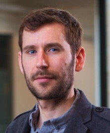 James M. LeBeau合作论文数Department of Materials Science and Engineering, Massachusetts Institute of Technology26
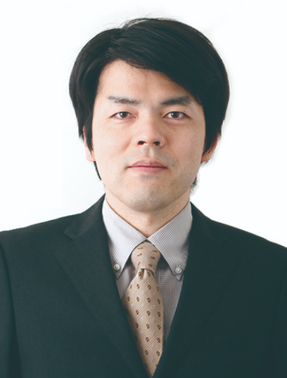 Teruyasu Mizoguchi (溝口照康)合作论文数Institute of Industrial Science, The University of Tokyo;Department of Materials Engineering, The University of Tokyo;National Institute of Science and Technology Policy25
 Ryo Ishikawa合作论文数Crystal Interface Laboratory, University of Tokyo21
 Stephen J Pennycook合作论文数Vanderbilt University;University of Tennessee;Department of Materials Science and Engineering, College of Design and Engineering, National University of Singapore21
 Stemmer Susanne合作论文数Departmrnt of Materials, College of Engineering, University of California, Santa Barbara20N.R. Lugg合作论文数School of Physics, University of Melbourne19
 Seki Takehito合作论文数Dept. of Materials Engineering &Science, University of Tokyo;Dept. of Materials Engineering & Science, University of Tokyo17Andrew R. Lupini合作论文数17
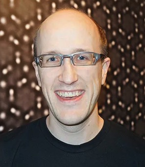 Colin Ophus合作论文数Department of Materials Science and Engineering, School of Engineering, Stanford University;Precourt Institute for Energy, Stanford Doerr School of Sustainability, Stanford University17Yuji Kohno合作论文数14
 Gabriel Sánchez-Santolino合作论文数Department of Materials Physics, Universidad Complutense de Madrid12
 Peter Nellist合作论文数Department of Materials, University of Oxford12Ciston Jim合作论文数Mol Foundry, Lawrence Berkeley Natl Lab12
 Takahisa Yamamoto合作论文数Graduate School of Engineering, Nagoya University12T. C. Petersen合作论文数11
 Joanne Etheridge合作论文数Department of Materials Science and Engineering, Faculty of Engineering, Monash University;Monash Centre for Electron Microscopy, Monash University10
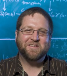 David Paganin合作论文数School of Physics and Astronomy, Monash University9
 Klaus van Benthem合作论文数Chemical Engineering and Materials Science Department, University of California-Davis9Daniel Joel Taplin合作论文数8
 Philipp M Pelz合作论文数University of California8
 Clark Laura合作论文数EMAT, University of Antwerp8
 Michael J Morgan合作论文数School of Physics, Monash University8
 Zhen Chen (陈震)合作论文数Institute of Physics, Chinese Academy of Sciences;University of Chinese Academy of Sciences8Eireann C Cosgriff合作论文数8
 Angus Kirkland合作论文数Department of Materials, University of Oxford;Rosalind Franklin Institute;Electron Physical Science Imaging Centre at Diamond Light Source8
 Ikuhara Yuichi合作论文数Institute of Engineering Innovation, University of Tokyo;WPI Advanced Institute for Materials Research, Tohoku University;Nanostructures Research Laboratory, Japan Fine Ceramics Center7Forbes Benjamin D.合作论文数7
 Takashi Taniguchi (谷口尚)合作论文数Research Center for Materials Nanoarchitectonics, National Institute for Materials Science;Graduate School of Science, Faculty of Science, Tohoku University7G. Behan合作论文数6
 Alireza Sadri合作论文数6
 Joseph Houston Dycus合作论文数6H Sawada合作论文数JEOL Ltd, Tokyo 1968558, Japan6
 Xiahan Sang (桑夏晗)合作论文数State Key Laboratory of Advanced Technology for Materials Synthesis and Processing, Wuhan University of Technology6Neish M J合作论文数6
 Rong Huang (黄荣)合作论文数School of Physics and Electronic Science, East China Normal University6
 Maria Varela合作论文数Materials Science and Technology Division, Oak Ridge National Laboratory;Complutense University of Madrid6Eiji Okunishi合作论文数6
 Bryan D Esser合作论文数Monash University;Monash Centre for Electron Microscopy6Christopher Witte合作论文数School of Physics;University of Melbourne;School of Physics, University of Melbourne6Troels Petersen合作论文数5S Azuma合作论文数5Mary Scott合作论文数Department of Materials Science and Engineering, University of California, Berkeley5




