The influence of minimal amounts of Ag (0.5-1.4 at%) on elemental distribution and crystalline quality of (Ag,Cu)(In,Ga)Se-2 (ACIGSe) absorbers grown by the three-stage coevaporation without added alkali elements is reported. The elemental ratios affect the amount of Ag to be uniformly incorporated into the chalcopyrite absorber and the open-circuit voltage (V-OC) of the ACIGSe solar cell devices. Ag-containing absorbers deposited at 530 degrees C achieve a best photoconversion efficiency of 18.2%. Due to an increased V-OC, ACIGSe absorbers perform better than their Ag-free variants at low deposition temperatures. The factors contributing to this increased V-OC of low-temperature devices are: 1) enhanced elemental Ga and In interdiffusion and hence their spatial distribution across the absorber thickness, leading to an increase in the minimum bandgap, 2) an improved absorber crystalline quality with larger grains resulting in high quasi-Fermi-level splitting and lower nonradiative losses. The photoluminescence data obtained on the ACIGSe absorbers reveal the corresponding variations in their bandgap and photoluminescence quantum yield. These material-level insights into Ag incorporation in chalcopyrite help to advance the development of chalcopyrite-based tandem solar cells, which-so far-is limited by the requirement of high deposition temperatures.
High‐efficiency Cu(In,Ga)Se 2 solar cells rely on Ga grading to mitigate back surface recombination. However, the inhomogeneous absorber has drawbacks, including increased non‐radiative loss and inadequate absorption. Therefore, literatures demand a paradigm shift of using a hole‐transport layer to passivate the back surface. Herein, a functional hole‐transport layer is demonstrated as an alternative to Ga grading. The novel hole‐transport layer is prepared as a double‐layer: co‐evaporated CuGaSe 2 covered by solution combustion synthesis prepared In 2 O 3 . As demonstrated by micrographs, elemental mapping, and photoluminescence spectroscopy, the oxide layer improves thermal stability and prevents Ga diffusion. However, during the absorber deposition, a complete ion exchange of In and Ga converts CuGaSe 2 /In 2 O 3 into CuInSe 2 /GaO x . Incorporating this hole‐transport layer in co‐evaporated nongraded CuInSe 2 solar cells leads to significantly increased minority carrier lifetime from 5 to 113 ns, yielding an 80 meV improvement in quasi‐Fermi‐level splitting. The devices exhibit improved open‐circuit voltage, as well as a promising fill factor of over 71%, indicating good hole‐transport properties. In these results, the passivation effect and good hole‐transport properties of the hole‐transport layer are experimentally demonstrated. Thus, high‐efficiency solar cells can be achieved by using a functional hole‐transport layer without relying on Ga grading.
While the current surging global energy crisis highlights the urgent need for a transition to renewable energy sources, the large physical footprint-as experienced by humans-of the required installations reduces public acceptance and therefore strongly hampers its development. Solar modules, for electricity and/or for heating, do not have the audible impact of wind turbines but their visible impact is currently prohibitive for many installation options, such as on the fa & ccedil;ades of buildings. Here we show that coatings of cholesteric liquid crystals (CLCs) can turn any black solar modules into passive surfaces with arbitrary colour or active surfaces with temperature sensitive colouration, yet with minimum loss of power conversion efficiency (PCE), thanks to their self-organized helical modulation generating structural colour. Most conspicuously, we combine red, green, and blue pixels to generate a non-spectral colour that blends into wooden or metallic backgrounds with a 50% relatively higher PCE than a ceramic ink equivalent since CLCs neither absorb nor scatter light. Further, we show thermochromic solar cells with colour tunable across the full visible spectrum, maintaining 88% of their original PCE. We argue these coatings can be developed to cover solar modules with either arbitrary full-colour images, allowing them to be aesthetically integrated into building fa & ccedil;ades and roofs in a way that is fully acceptable by the public, or with active colour changing to add functional value, while always keeping high PCE.
The Shockley-Queisser (SQ) theorem predicts the theoretical upper limit of the VOC in a solar cell with a step like absorptance A(E) function, where A(E) is one above the band gap and zero below it. However, real solar cells do not show a step like absorption spectrum. Consequently, the maximum achievable VOC known as radiative limit is below the SQ limit. In this study we investigate the maximum achievable voltage for two types of samples: CuInSe2 with a uniform band gap profile and Cu(In, Ga)Se 2 with a band gap gradient. The absorptance spectra for these samples are extracted from a combination of photoluminescence (PL) and transmittance/reflectance measurements. Subsequently, the extracted absorptance is utilized to calculate the radiative voltage losses for each sample. Gaussian fitting to the derivative of the absorptance spectrum is used to extract the effective band gap from the maximum and the broadening parameter of the band gap distribution (σg). The findings reveal that Cu(In, Ga)Se 2 samples with a band gap gradient exhibit higher values for bradening (σg) and increased radiative voltage loss compared to samples without a band gap gradient. Furthermore, simulations are conducted by defining the A(E) spectrum as an error function. These simulation results demonstrate the correlation between the increase in radiative voltage loss and the rise in σg.
The presence of Urbach tails in Cu(In,Ga)Se-2 (CIGSe) absorbers has been identified as a limiting factor for the performance of the CIGSe solar cells. The tail states contribute to both radiative and non-radiative recombination processes, ultimately leading to a reduction in the open-circuit voltage and, consequently, decreasing the overall efficiency of CIGSe devices. Urbach tails result from structural and thermal disorders. The Urbach tails can be characterized by the Urbach energy, which is associated with the magnitude of the tail states. Within polycrystalline CIGSe absorbers, grain boundaries can be considered as structural disorder and, therefore, can potentially contribute to the Urbach tails. In fact, it has been proposed that the band bending at grain boundaries contribute significantly to the tail states. This study focuses on examining the correlation between Urbach tails and the band bending at the grain boundaries. The Urbach energies of the CIGSe samples are extracted from photoluminescence (PL) measurements, which reveal that the introduction of Sodium (Na) into the material can lead to a reduction in the Urbach energy, and an even further decrease can be achieved through the RbF post-deposition treatment. The band bending at the grain boundaries is investigated by Kelvin probe force microscopy measurements. A thorough statistical analysis of more than 340 grain boundaries does not show any correlation between Urbach tails and grain boundaries. We measure small band bending values at the grain boundaries, in the range of the thermal energy (26 meV at room temperature). Furthermore, our intensity dependent PL measurements indicate that Urbach tails are, at least in part, a result of electrostatic potential fluctuations. This supports the model that the introduction of alkali elements mainly decreases the magnitude of electrostatic potential fluctuations, resulting in a subsequent reduction in the Urbach energy.
Alkali metal doping and grain boundaries (GB) have been at the center of attention within the Cu(In,Ga)(S,Se) 2 photovoltaics community for years. This study provides the first experimental evidence that the GB of sodium‐doped CuInSe 2 thin films may undertake reversible oxidation even at room temperature, whereas undoped films may not. The findings are corroborated by cathodoluminescence imaging, secondary ion mass spectrometry, and Kelvin probe force microscopy on air‐exposed films subsequently subject to vacuum. A thermochemical assessment identifies the likely solid–gas equilibria involved. These reactions open new research questions with respect to the beneficial role played by alkali metal dopants in chalcopyrite solar cells and may steer the community toward new breakthroughs.
Urbach tails describe a density of states that decays exponentially into the band gap. Non-radiative and radiative recombinations in the Urbach tails contributes to voltage loss in the Cu(In, Ga)Se2 CIGSe solar cells. In the CIGSe semiconductor, the Urbach tails can be suppressed by alkali fluoride post-deposition treatment (PDT). We report the impact of NaF and KF-PDT on the quasi-Fermi level splitting (QFLS) and Urbach energy of the CIGSe absorbers, which are evaluated by absolute photoluminescence measurement. Our data reveal that both NaF and KF PDT have beneficial impacts on the QFLS. Samples with a low Na concentration show high Urbach energies, which are decreased by NaF-PDT. Sufficient KF PDT on the samples deposited on Mo-coated soda lime glass (i.e., with a high concentration of Na) further decreases the Urbach energy. The improvement of the QFLS is not solely due to the reduction of tail states, but it can also be due to surface passivation, grain boundary passivation or increase in the doping concentration.
Chemically processed methylammonium tin-triiodide (CH3NH3SnI3) films include Sn in different oxidation states, leading to poor stability and low power conversion efficiency of the resulting solar cells (PSCs). The development of absorbers with Sn [2+] only has been identified as one of the critical steps to develop all Sn-based devices. Here, we report on coevaporation of CH3NH3I and SnI2 to obtain absorbers with Sn being only in the preferred oxidation state [+2] as confirmed by X-ray photoelectron spectroscopy. The Sn [4+]-free absorbers exhibit smooth highly crystalline surfaces and photoluminescence measurements corroborating their excellent optoelectronic properties. The films show very good stability under heat and light. Photoluminescence quantum yields up to 4 × 10⁻³ translate in a quasi Fermi-level splittings exceeding 850 meV under one sun equivalent conditions showing high promise in developing lead-free, high efficiency, and stable PSCs.
Absolute photoluminescence measurements present a tool to predict the quality of photovoltaic absorber materials before finishing the solar cells. Quasi Fermi level splitting predicts the maximal open circuit voltage. However, various methods to extract quasi Fermi level splitting are plagued by systematic errors in the range of 10-20 meV. It is important to differentiate between the radiative loss and the shift of the emission maximum. They are not the same and when using the emission maximum as the "radiative" band gap to extract the quasi Fermi level splitting from the radiative efficiency, the quasi Fermi level splitting is 10 to 40 meV too low for a typical broadening of the emission spectrum. However, radiative efficiency presents an ideal tool to compare different materials without determining the quasi Fermi level splitting. For comparison with the open circuit voltage, a fit of the high energy slope to generalised Planck's law gives more reliable results if the fitted temperature, i.e. the slope of the high energy part, is close to the actual measurement temperature. Generalised Planck's law also allows the extraction of a non-absolute absorptance spectrum, which enables a comparison between the emission maximum energy and the absorption edge. We discuss the errors and the indications when they are negligible and when not.
Organic-inorganic hybrid perovskite solar cells (PSCs) achieved already more than 25% power conversion efficiency making them one of the fastest-growing solar cell technologies. However, most state-of-art PSCs employ lead (Pb) as a "B" cation in the ABX3 type crystalline absorbers. Sn has been considered to be a potential replacement for Pb. However, chemically processed Sn-perovskite films often exhibit a high number of Sn vacancies and a high density of Sn4+ species, leading to poor stability and low power conversion efficiency of the tin-based PSCs. Herein we report co-evaporation of CH3NH3I and SnI2 to obtain Sn4+-free CH3NH3SnI3 perovskite films with excellent optoelectronic properties and improved stability. XRD measurements confirm the polycrystalline films, mainly oriented in the (100) plane of a cubic crystal. XPS analysis confirms that the films consist of Sn only in the 2+ oxidation state. AFM and KPFM analysis reveal smooth topology and uniform surface workfunction. The films show very good stability under heating and photodegradation confirmed by XRD and photoluminescence (PL) degradation measurements. The co-evaporated CH3NH3SnI3 films exhibit PL quantum yields up to 9x10⁻⁴ translating in a quasi Fermi-level splitting of 844 meV under one sun equivalent conditions. Extracted low values of Urbach energies (16 meV) suggest that the films exhibit a low number of defects near the band edges showing high promise in developing lead-free, high efficiency, and stable PSCs.
This work focused on the spray pyrolysis deposition of Cu2SnS3 (CTS) thin films using a stable basic solution. The effect of the most important parameters including the substrate temperature and copper concentration on the structural, optical and electrical properties of as-deposited thin films was investigated. Qualified thin films with suitable microstructure and composition could be deposited at 370celcius. XRD and Raman analysis while confirming the pure CTS film formation, show that as the Cu/Sn decreases, the crystal structure layers are changed from the tetragonal phase to the cubic phase mixed with Sn-rich phases. The optical study shows its band gap between 1.08 and 1.2 eV for different Cu/Sn ratios with the absorption coefficient being more than104 cm 1. The Hall and Mott-Schottky measurements reveal that all samples show a p-type behavior and carrier concentration of the samples rise as the Cu/Sn ratio is enhanced. A full spray superstrate solar cell based on CTS (Cu/Sn = 1 with a semiconductor behavior) resulted in an efficiency of 0.63%.
 Susanne Siebentritt合作论文数Department of Physics and Materials Science, Faculty of Science, Technology and Medicine, University of Luxembourg7
 Michele Melchiorre合作论文数5
 Phillip J. Dale合作论文数4Taowen Wang合作论文数3Ricardo G. Poeira合作论文数3
 Alex Redinger合作论文数II. Physikalisches Institut, Universität zu Köln3Muhammad Uzair Farooq合作论文数2
 Himanshu Phirke合作论文数2
 Aubin JC. M. Prot合作论文数2
 Ajay Singh合作论文数2
 Mohit Sood合作论文数Dept Phys & Mat Sci, Univ Luxembourg2
 Hakam Agha合作论文数Max Planck Inst Dynam & Selforg, Fassberg 17, D-37077 Gottingen, Germany2
 Hasan A. Yetkin合作论文数Technical University Berlin2
 Yan-Song Zhang合作论文数Dept Photon, Natl Cheng Kung Univ2
 Jeremy Hieulle合作论文数Energy Mat & Surface Sci Unit EMSSU, Okinawa Inst Sci & Technol Grad Univ OIST2
 Rijeesh Kizhakidathazhath合作论文数Phys & Mat Sci Res Unit, Univ Luxembourg2N. Valle合作论文数2
 Christian Kaufmann合作论文数Institut Kompetenz-Zentrum Photovoltaik Berlin, Humboldt-Universität zu Berlin2
 Jan Peter Felix Lagerwall合作论文数Physics & Materials Science Research Unit, University of Luxembourg2Pablo Reyes-Figueroa合作论文数1Jakob Lauche合作论文数1Joana Ferreira Machado合作论文数1
 Anastasiya Zelenina合作论文数1
 Maryam Heidariramsheh合作论文数Inst Nanosci & Nanotechnol INST, Sharif Univ Technol1
 Longfei Song合作论文数Materials Research and Technology Department, Luxembourg Institute of Science and Technology (LIST)1Jose Virtuoso合作论文数1
 Deepanjan Sharma合作论文数1
 Weiwei Zuo合作论文数University of Stuttgart1
 Finn Babbe合作论文数Lawrence Berkeley National Laboratory1Ajay S. Singh合作论文数1Damilola Adeleye合作论文数Lab Photovolta, Univ Luxembourg1Nikolaus Weinberger合作论文数1
 Nicoleta Nicoara合作论文数Int Iberian Nanotechnol Lab INL, P-4715330 Braga, Portugal1Harvey Guthrey合作论文数Nat. Renewable Energy Lab.;c;Nat. Renewable Energy Lab.1
 Defay, Emmanuel合作论文数CEA LETI1
 Thomas Paul Weiss合作论文数Laboratory for Photovoltaics, University of Luxembourg1
 Michael Saliba合作论文数Institute for Photovoltaics, University of Stuttgart;Forschungszentrum Jülich1
 Uwe Rau合作论文数Institut für Energie- und Klimaforschung, Forschungszentrum Jülich GmbH1
 Diego Colombara合作论文数Phys & Mat Sci Res Unit, Univ Luxembourg1
 Seyed Mohammad Mahdavi合作论文数Institute for Nanoscience and Nanotechnology (INST),, Sharif University of Technology1Damien Aureau合作论文数1Sascha Sadewasser合作论文数Hahn-Meitner-Institut1
 Sebastjan Glinsek合作论文数1
 Rutger Schlatmann合作论文数Solar Cells R&D, Helianthos bv1
 Iver Lauermann合作论文数Hahn-Meitner-Institut Berlin GmbH1
 Hossam Elanzeery合作论文数1
 Nima Taghavinia合作论文数Physics Department, Sharif University of Technology1
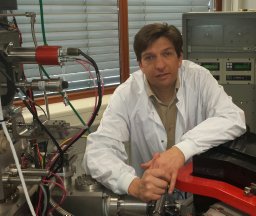 Jean-Nicolas Audinot合作论文数Institut de chimie de la matière condensée de Bordeaux, CNRS1
 Tom Wirtz合作论文数Department “Science and Analysis of Materials” (SAM), Centre de Recherche Public – Gabriel Lippmann, 41 rue du Brill, L-4422 Belvaux, Luxembourg1




