Fast and accurate detection of light in the near-infrared (NIR) spectral range plays a crucial role in modern society, from alleviating speed and capacity bottlenecks in optical communications to enhancing the control and safety of autonomous vehicles through NIR imaging systems. Several technological platforms are currently under investigation to improve NIR photodetection, aiming to surpass the performance of established III-V semiconductor p-i-n (PIN) junction technology. These platforms include in situ-grown inorganic nanocrystals and nanowire arrays, as well as hybrid organic-inorganic materials such as graphene-perovskite heterostructures. However, challenges remain in nanocrystal and nanowire growth, large-area fabrication of high-quality 2D materials, and the fabrication of devices for practical applications. Here, we explore the potential for tailored semiconductor nanocrystals to enhance the responsivity of planar metal-semiconductor-metal (MSM) photodetectors. MSM technology offers ease of fabrication and fast response times compared to PIN detectors. We observe enhancement of the optical-to-electric conversion efficiency by up to a factor of ~2.5 through the application of plasmonically-active semiconductor nanorods and nanocrystals. We present a protocol for synthesizing and rapidly testing the performance of non-stoichiometric tungsten oxide (WO$_{3-x}$) nanorods and cesium-doped tungsten oxide (Cs$_y$WO$_{3-x}$) hexagonal nanoprisms prepared in colloidal suspensions and drop-cast onto photodetector surfaces. The results demonstrate the potential for a cost-effective and scalable method exploiting tailored nanocrystals to improve the performance of NIR optoelectronic devices.
Dopant-free lateral p-n junctions in the GaAs/AlGaAs material system have attracted interest due to their potential use in quantum optoelectronics (e.g., optical quantum computers or quantum repeaters) and ease of integration with other components, such as single electron pumps and spin qubits. A major obstacle to integration has been unwanted charge accumulation at the p-n junction gap that suppresses light emission, either due to enhanced non-radiative recombination or inhibition of p-n current. Typically, samples must frequently be warmed to room temperature to dissipate this built-up charge and restore light emission in a subsequent cooldown. Here, we introduce a practical gate voltage protocol that clears this parasitic charge accumulation, in-situ at low temperature, enabling the indefinite cryogenic operation of devices. This reset protocol enabled the optical characterization of stable, bright, dopant-free lateral p-n junctions with electroluminescence linewidths among the narrowest (< 1 meV; < 0.5 nm) reported in this type of device. It also enabled the unambiguous identification of the ground state of neutral free excitons (heavy and light holes), as well as charged excitons (trions). The free exciton emission energies for both photoluminescence and electroluminescence are found to be nearly identical (within 0.2 meV or 0.1 nm). The binding and dissociation energies for free and charged excitons are reported. A free exciton lifetime of 237 ps was measured by time-resolved electroluminescence, compared to 419 ps with time-resolved photoluminescence.
In this research, we presents a novel design for an all-electrical single photon emitter that utilizes a single electron pump and a lateral p-n junction based on an AlGaAs/GaAs heterostructure. The fundamental promise of single photon emission is achieved by injecting one and only one electron into the p-n junction, where one photon is generated after e-h radiative recombination. This ensures an intrinsically on-demand and deterministic single photon source. Up to GHz repetition rate is expected given the single electron pump has demonstrated quantized generation of electrons in the GHz range. We will present some promising stable EL emission after overcoming the charge accumulation problem in our dopant-free architecture.
Illumination is performed at low temperature on dopant-free two-dimensional electron gases (2DEGs) of varying depths, under unbiased (gates grounded) and biased (gates at a positive or negative voltage) conditions. Unbiased illuminations in 2DEGs located more than 70 nm away from the surface result in a gain in mobility at a given electron density, primarily driven by the reduction of background impurities. In 2DEGs closer to the surface, unbiased illuminations result in a mobility loss, driven by an increase in surface charge density. Biased illuminations performed with positive applied gate voltages result in a mobility gain, whereas those performed with negative applied voltages result in a mobility loss. The magnitude of the mobility gain (loss) weakens with 2DEG depth, and is likely driven by a reduction (increase) in surface charge density. Remarkably, this mobility gain/loss is fully reversible by performing another biased illumination with the appropriate gate voltage, provided both $n$-type and $p$-type Ohmic contacts are present. Experimental results are modeled with Boltzmann transport theory, and possible mechanisms are discussed.
B. Buonacorsi, 2 F. Sfigakis, 3, 4, a) A. Shetty, 4 M. C. Tam, 6 H. S. Kim, 6 S. R. Harrigan, 2, 6 F. Hohls, M. E. Reimer, 2, 3, 5 Z. R. Wasilewski, 2, 3, 5, 6 and J. Baugh 2, 3, 4, 6, b) Institute for Quantum Computing, University of Waterloo, Waterloo N2L 3G1, Canada Department of Physics, University of Waterloo, Waterloo N2L 3G1, Canada Northern Quantum Lights Inc., Waterloo N2B 1N5, Canada Department of Chemistry, University of Waterloo, Waterloo N2L 3G1, Canada Department of Electrical and Computer Engineering, University of Waterloo, Waterloo N2L 3G1, Canada Waterloo Institute for Nanotechnology, University of Waterloo, Waterloo N2L 3G1, Canada Physikalisch-Technische Bundesanstalt (PTB), 38116 Braunschweig, Germany
Illumination is performed at low temperature on dopant-free two-dimensional electron gases (2DEGs) of varying depths, under unbiased (gates grounded) and biased (gates at a positive or negative voltage) conditions. Unbiased illuminations in 2DEGs located more than 70 nm away from the surface result in a gain in mobility at a given electron density, primarily driven by the reduction of background impurities. In 2DEGs closer to the surface, unbiased illuminations result in a mobility loss, driven by an increase in surface charge density. Biased illuminations performed with positive applied gate voltages result in a mobility gain, whereas those performed with negative applied voltages result in a mobility loss. The magnitude of the mobility gain (loss) weakens with 2DEG depth, and is likely driven by a reduction (increase) in surface charge density. Remarkably, this mobility gain/loss is fully reversible by performing another biased illumination with the appropriate gate voltage, provided both n-type and p-type ohmic contacts are present. Experimental results are modeled with Boltzmann transport theory, and possible mechanisms are discussed.
Nonpolar a-plane GaN epitaxial films were grown on an r-plane sapphire using the plasma-assisted molecular beam epitaxy system, with various nitrogen plasma power conditions. The crystallinity of the films was characterized by high-resolution Xray diffraction and reciprocal space mapping. Using the X-ray "rocking curve-phi scan", [0002],[1-100], and [1-102] azimuth angles were identified, and interdigitated electrodes along these directions were fabricated to evaluate the direction-dependent UV photoresponses. UV responsivity (R) and internal gain (G) were found to be dependent on the azimuth angle and in the order of [0002] > [1-102] > [1-100], which has been attributed to the enhanced crystallinity and lowest defect density along [0002] azimuth. The temporal response was very stable irrespective of growth conditions and azimuth angles. Importantly, response time, responsivity, and internal gain were 210 ms, 1.88 A W-1, and 648.9%, respectively, even at a bias as low as 1 V. The results were validated using the Silvaco Atlas device simulator, and experimental observations were consistent with simulated results. Overall, the photoresponse is dependent on azimuth angles and requires further optimization, especially for materials with in-plane crystal anisotropy.
Piezoelectric energy harvesting systems are used to convert vicinity vibrations into useful electrical energy. Effect of various shapes and materials open the gateway towards the choice of maximum power generation for the micro and nano world. Comsol Multiphysics was used to simulate the four designed shapes named as Pi, E, Rectangular and T in the size range of less than hum but greater than 1 micron. Designed shapes worked under the impact of ambient vibrations using few piezoelectric materials for the maximum power generation so that traditional power sources can be replaced with such piezoelectric energy harvester. A layer of piezoelectric material (PZT-511, AN, BaTiO3) of thickness 0.5 pm is added to the cantilever and the base material is silicon of thickness 1.5 p.m. Simulations were performed using the piezoelectric device module of Comsol Multiphysics. All three materials were studied for the all four cantilever geometries. The generated power was observed maximum as 382.5 mu W in case of the barium titanate material with rectangular shape geometry but the displacement is 0.132 mu m which is very less whereas E shape cantilever shows the maximum displacement of 0.6078 pin in case of PZT-5H, Hence rectangular shape with barium titanate material is concluded to be good for maximum power generation but the displacement factor cannot be neglected, hence the cantilever with E shape geometry is considered as the best with a generated power of 49.005 mu W and a displacement of 0.6078 mu m.
This paper presents the simulation studies of Metal-Semiconductor-Metal (MSM) Photodetector (PD) with and without plasmonic enhancement. The simulations were carried out using COMSOL Multiphysics (R) software. The semiconductor layer was p-type ZnO with a doping concentration of 10(16)/cm(3). The plasmonic layer was of Au nanoparticles. The PD was irradiated with 10W UV radiation of wavelength 280nm. The output currents of MSM PD with and without plasmonic layer were found to be similar to 0.9x10(-7)A and similar to 0.8x10(-8)A respectively. It was observed that there is an appreciable increase (factor of 10) in photo current in devices with a plasmonic layer. The effect of change in the size of Au nano particles on output photocurrent was also studied.
Self-assembled InN quantum dots (QDs) were grown on Si(111) substrate using plasma assisted molecular beam epitaxy (PA-MBE). Single-crystalline wurtzite structure of InN QDs was confirmed by X-ray diffraction. The dot densities were varied by varying the indium flux. Variation of dot density was confirmed by FESEM images. Interdigitated electrodes were fabricated using standard lithog- raphy steps to form metal-semiconductor-metal (MSM) photodetector devices. The devices show strong infrared response. It was found that the samples with higher density of InN QDs showed lower dark current and higher photo current. An explanation was provided for the observations and the experimental results were validated using Silvaco Atlas device simulator.
This paper reports an improvement in Pt/n-GaN metal-semiconductor (MS) Schottky diode characteristics by the introduction of a layer of HfO2 (5 nm) between the metal and semiconductor interface. The resulting Pt/HfO2/n-GaN metal-insulator-semiconductor (MIS) Schottky diode showed an increase in rectification ratio from 35.9 to 98.9(@ 2V), increase in barrier height (0.52 eV to 0.63eV) and a reduction in ideality factor (2.1 to 1.3) as compared to the MS Schottky. Epitaxial n-type GaN films of thickness 300nm were grown using plasma assisted molecular beam epitaxy (PAMBE). The crystalline and optical qualities of the films were confirmed using high resolution X-ray diffraction and photoluminescence measurements. Metal-semiconductor (Pt/n-GaN) and metal-insulator-semiconductor (Pt/HfO2/n-GaN) Schottky diodes were fabricated. To gain further understanding of the Pt/HfO2/GaN interface, I-V characterisation was carried out on the MIS Schottky diode over a temperature range of 150 K to 370 K. The barrier height was found to increase (0.3 eV to 0.79 eV) and the ideality factor decreased (3.6 to 1.2) with increase in temperature from 150 K to 370 K. This temperature dependence was attributed to the inhomogeneous nature of the contact and the explanation was validated by fitting the experimental data into a Gaussian distribution of barrier heights.
Micro-electromechanical systems (MEMS) piezoelectric harvester provides alternative power sources. Energy harvesting is utilized in power generator with characteristics length of less then 1 mm and more then 1 micron. The cantilever geometries have been made using Structure mechanics module for generated power. The piezoelectric material (PZT-5H) with thickness of 0.5 μm and silicon as base material with thickness 1.5 μm is added to cantilever using piezoelectric devices module. Among various shapes like (E,pi,T) though which E shaped cantilever shows the greatest deflection of 0.6078 μm and the power as 49.05 μW, whereas the T and pi shaped cantilever gives less piezoelectric voltage.
Gallium nitride (n-type) films of thickness 300nm were grown on c-plane sapphire substrates using plasma assisted molecular beam epitaxy (PA-MBE). High resolution X-ray diffraction and photoluminescence measurements were used to confirm the crystalline and optical qualities of the grown films. Metal-semiconductor Schottky diodes were fabricated using Pt as the Schottky metal and Al as the Ohmic metal contact. Metal-insulator-semiconductor Schottky diodes were also fabricated using HfO 2 (10nm) as the insulator material. Diode parameters like barrier height and ideality factor were extracted from I-V measurements. Introduction of HfO 2 as the insulator layer leads to better rectifying behavior (forward to reverse current ratio improves from 5.1 to 8.9) with a reduction in reverse leakage current (by 7.4 times), increase in barrier height (from 0.62eV to 0.74eV) and a reduction in ideality factor (from 6 to 4.1) of the Schottky diode.
Nonpolar a-GaN (11-20) epilayers were grown on r-plane (1-102) sapphire substrates using plasma assisted molecular beam epitaxy. High resolution x-ray diffractometer confirmed the orientation of the grown film. Effect of the Ga/N ratio on the morphology and strain of a-GaN epilayers was compared and the best condition was obtained for the nitrogen flow of 1 sccm. Atomic force microscopy was used to analyze the surface morphology while the strain in the film was quantitatively measured using Raman spectroscopy and qualitatively analyzed by reciprocal space mapping technique. UV photo response of a-GaN film was measured after fabricating a metal-semiconductor-metal structure over the film with gold metal. The external quantum efficiency of the photodetectors fabricated in the (0002) polar and (11-20) nonpolar growth directions were compared in terms of responsivity and nonpolar GaN showed the best sensitivity at the cost of comparatively slow response time.
200 nm thick films of gallium nitride were grown on sapphire substrate using molecular beam epitaxy. Gold nanoparticles were fabricated on the grown films by thermal evaporation followed by annealing. Aluminium nanostructures were fabricated on another set of films using nanosphere lithography. Interdigited electrodes were fabricated using standard lithography to form metal-semiconductor-metal photodetectors. The performance of bare gallium nitride films were compared with the samples that had Au nanoparticles and Al nanostructures. An enhancement of the photocurrent with negligible change in dark current was observed in both cases.
Introduction: Energy harvesting is an emerging area of research where wasted ambient energy is converted into useful electrical power thus providing a promising solution to the environmental issues associated with battery powered systems [1-3]. Among the various sources of ambient energy, vibration based energy harvesting is one of the popular choices. MEMS based microcantilevers have been a popular choice for vibration based energy harvesting [4-6]. The deflection of a cantilever for a particular applied force depends on the stiffness of the cantilever and its spring constant. A lower stiffness and a lower value of spring constant would result in greater deflection for a particular value of applied force [7]. In sensing applications, we would ideally like to get maximum deflection for minimum change in the value of the quantity being sensed. Hence, for sensing applications, cantilevers with greater sensitivity are preferred [8,9]. A layer of piezoelectric material (ZnO, AlN and PZT are modeled) is added to the cantilever and using COMSOL Multiphysics' Piezoelectric Devices physics, we determine the piezoelectric voltage that is generated in each of these cases. Use of COMSOL Multiphysics: We use COMSOL Multiphysics' Piezoelectric Devices physics to numerically solve for the various cantilever geometries and compare the obtained deflection, stress and generated piezoelectric voltage. We study four geometries namely, conventional rectangular cantilever, pi -shaped cantilever, T shaped cantilever and finally a triangular cantilever. Properties of Si and the piezoelectric layer (ZnO, AlN and PZT are modeled) are taken from the COMSOL material library. One of the cantilever ends is assigned a fixed boundary condition and the other ends are given a free boundary condition. We keep the bottom of the piezoelectric layer as ground and assign a floating potential condition to the top surface of the piezoelectric layer. A constant force of 0.5μN is applied on the ends of all the cantilevers. The applied force results in a deflection in the cantilever. The deflection creates a stress in the piezoelectric layer and this stress generates a voltage in a direction perpendicular to the stress (d31 mode). The displacement, stress created and the generated piezoelectric voltages are compared for various geometries. Results: We observe a greater deflection in the triangular and T shaped cantilevers as compared to the conventional cantilever (Figure 1). The greater deflection results in a greater stress and strain in the piezoelectric layer resulting in greater generated piezoelectric voltage (Figure 2). Thus we observe that the triangular geometry is most suitable for piezoelectric based energy harvesting cantilevers (1.89 times higher voltage as compared to conventional cantilever) followed by T shaped cantilevers. The regular geometry cantilever based energy harvester has already been fabricated and characterized under the Indian Nanoelectronics Users Program (INUP) at Centre for Nano Science and Engineering (CeNSE), IISc, Bangalore. Those results have been reported in an earlier work [10]. In the future, we would like to validate our theoretical and simulation studies by the fabrication and characterization of the designed devices with non-conventional geometries.
Introduction: III-nitride semiconductors in general and gallium nitride in particular have recently become increasingly important for optoelectronic applications like LEDs, solar cells and photodetectors [1-3] due to their attractive properties like wide and direct bandgap, high power handling capability and high breakdown field. GaN as a choice of semiconductor material for UV detectors has gained prominence recently due to advantages like small size and good thermal and chemical stability, and wide bandgap [4]. Among the various photodetector structures, the planar MSM structure has advantages like ease of fabrication, inherently low capacitance and consequently, greater receiver sensitivity as compared to other vertically structured photodetectors. Experimental Details: This paper studies the improvement of photocurrent properties obtained by the presence of Au nanoparticles in between the electrode fingers. Nanoplasmonic enhancement of photodetectors by scattering effects has been well known [5,6] and is considered as an effective way of improving the photo current characteristics of a photodetector. There have been studies in literature on the use of plasmonics beyond the visible and into the UV [7] and IR [8-9] part of the spectrum. There has been a study on the use of Ag nanoparticles for the enhancement of UV photoresponse of a GaN MSM photodetector [10]. In that work, the use of Ag had resulted in a slight reduction in Schottky barrier height at the electrode-GaN interface. Ag and Au being the most commonly used plasmonic materials; in this study we explore the use of Au instead of Ag for nanoplasmonic enhancement. Au has a higher electron affinity than Ag and we expect that it will provide better interface characteristics than Ag at the electrode-GaN interface with little or no reduction in scattering efficiency. Samples used in this work consist of commercially obtained, MOCVD grown, undoped GaN films on c-plance sapphire substrates. This is followed by deposition of a 5nm film of Au on the GaN film using thermal evaporation. This is followed by annealing in nitrogen ambient at 400°C for 30 minutes. SEM images (Figure 1) after annealing confirmed the formation of Au nanoparticles. The sizes of the particles are found to vary from 40nm to 80nm. This is followed by fabrication of interdigited electrodes to form the MSM photodetector structure (Figure 2). A UV lamp with a spectral range of 300nm to 400nm was used as the source of UV illumination. The dark and photocurrent measurements were made using a probe station and an Agilent B1500A Device Analyzer. Use of COMSOL Multiphysics®: The photodetector with plasmonic effects has been modeled using the RF Module along with the newly introduced Semiconductor Module of COMSOL Multiphysics®. COMSOL was chosen for the modeling as it enables us to couple solutions of Maxwell's equations (required to model the plasmonics effects) with the solutions to carrier continuity equations under illumination (required to model the actual photodetector). Results: The simulations results agree well with experimental results and we obtain an increase of photocurrent of upto 1.4 times in the presence of the Au nanoparticles (Figure 3)
 Saluru Baba Krupanidhi合作论文数Materials Research Centre, Indian Institute of Science8
 Jonathan Baugh合作论文数Institute for Quantum Computing;University of Waterloo;Institute for Quantum Computing, University of Waterloo8
 Basanta Roul合作论文数Central Research Laboratory, Bharat Electronics7
 Francois Sfigakis合作论文数Institute for Quantum Computing, University of Waterloo;Department of Chemistry, University of Waterloo7
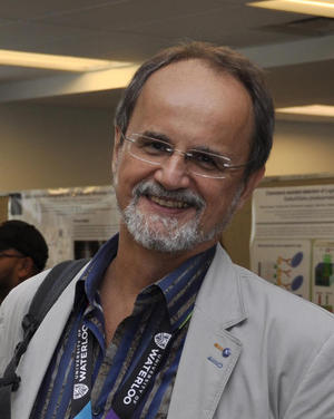 Zbigniew Wasilewski合作论文数Department of Physics and Astronomy, University of Waterloo7
 Brandon Buonacorsi合作论文数Inst Quantum Comp, Univ Waterloo6
 K. J. Vinoy合作论文数Microwave Laboratory;ECE Department;Indian Institute of Science Bangalore;Microwave Laboratory, Indian Institute of Science Bangalore6
 greeshma chandan合作论文数Dept Mat Sci & Engn, Univ Delaware5
 Michael Reimer合作论文数Department of Electrical and Computer Engineering, Engineering School, University of Waterloo;Quantum Photonic Devices Laboratory, Institute for Quantum Computing, University of Waterloo5
 Priya Chhabra合作论文数4
 shruti mukundan合作论文数Materials Research Centre, Indian Institute of Science4
 lokesh mohan合作论文数Materials Research Centre, Indian Institute of Science4M. C. Tam合作论文数3
 HoSung Kim合作论文数3A. F. Croxall合作论文数2Sara Hosseini合作论文数2Brad van Kasteren合作论文数2Man Chun Tam合作论文数2Nachiket Sherlekar合作论文数2Pinki Graak合作论文数2
 Ankit Gupta合作论文数2D. Austing合作论文数2Zach Merino合作论文数2W. Y. Mak合作论文数2H. S. Kim合作论文数2
 Ian Farrer合作论文数Department of Electronic and Electrical Engineering, Faculty of Engineering, The University of Sheffield2
 Michael Pepper合作论文数Department of Electronic and Electrical Engineering, University College London2
 Harvey Beere合作论文数Semiconductor Physics Group, University of Cambridge2
 Mahesh Kumar合作论文数Surface Science, Ultrafast Optoelectronics & THz Photonics Lab, National Physical Laboratory, Council of Scientific and Industrial Research;Academy of Scientific and Innovative Research2
 K.Das Gupta合作论文数Department of Physics, Indian Institute of Science2
 A Sachrajda合作论文数National Research Council Canada2Frank Hohls合作论文数Institut fur Festkorperphysik;Universitat Hannover;Institut fur Festkorperphysik, Universitat Hannover2
 Alexander Hamilton合作论文数School of Physics, Faculty of Science, The University of New South Wales;ARC Centre of Excellence in Future Low-Energy Electronics Technologies2
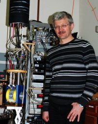 Sergei a Studenikin合作论文数Institute for Microstructural Sciences;National Research Council of Canada;Institute for Microstructural Sciences, National Research Council of Canada2D. Kumar合作论文数1S. Kaur合作论文数1Dinesh Kumar合作论文数1Eduardo Barrera合作论文数1A Gupta合作论文数1
 Chris Deimert合作论文数University of Waterloo1
 Stephen R. Harrigan合作论文数Inst Quantum Comp, Univ Waterloo1Lin Tian合作论文数1Alan Tam合作论文数1
 Nazia Fathima合作论文数Centre for Nano Science and Engineering, Indian Institute of Science1
 Rohit Pant合作论文数Mat Res Ctr, Indian Inst Sci1
 Jyothi Balakrishnan合作论文数1
 Ambarish Ghosh合作论文数1Kamal John Sundar合作论文数1Ubbelohde Niels合作论文数1




