Low-dimensional van der Waals materials have been extensively studied as a platform with which to generate quantum effects. Advancing this research, topological quantum materials with van der Waals structures are currently receiving a great deal of attention. Here, we use the concept of designing topological materials by the van der Waals stacking of quantum spin Hall insulators. Most interestingly, we find that a slight shift of inversion centre in the unit cell caused by a modification of stacking induces a transition from a trivial insulator to a higher-order topological insulator. Based on this, we present angle-resolved photoemission spectroscopy results showing that the real three-dimensional material Bi4Br4 is a higher-order topological insulator. Our demonstration that various topological states can be selected by stacking chains differently, combined with the advantages of van der Waals materials, offers a playground for engineering topologically non-trivial edge states towards future spintronics applications.
Recent progress in understanding the electronic band topology and emergent topological properties encourage us to reconsider the band structure of well-known materials including elemental substances. Controlling such a band topology by external field is of particular interest from both fundamental and technological viewpoints. Here we report possible signatures of the pressure-induced topological phase transition from a semiconductor to a Weyl semimetal in elemental tellurium probed by transport measurements. Pressure variation of the periods of Shubnikov-de Haas oscillations, as well as oscillation phases, shows an anomaly around the pressure theoretically predicted for topological phase transition. This behavior is consistent with the pressure-induced band deformation and resultant band-crossing effect. Moreover, effective cyclotron mass is reduced toward the critical pressure, potentially reflecting the emergence of massless linear dispersion. The present result paves the way for studying the electronic band topology in well-known compounds and topological phase transition by the external field.
グラフェンや MoS2 などと同様に、黒リンは2次元原子膜が積層した構造をもつ。バルクでは 0.3 eVの直接遷移型バンドギャップをもつことや、積層枚数により単層の 2 eVまでバンドギャッ プを調整できる可能性があること、大きな移動度が報告されていることなどから、ポスト・グラ フェン候補として黒リンへ次世代電子デバイス材料としての期待が高まっている。加えて、黒リ ンの電気伝導性は圧力印加で大きく変化し、大気圧での半導体的振る舞いから 1 GPa程度の高圧 下で金属化することや、10 GPa程度で超伝導が発現することも分かっている。更に、半導体-金 属転移に際しては、グラフェンに類似したディラック電子状態を3次元(バルク)で持つことや、 バンド反転してトポロジカル絶縁体状態が発現することなども予想されており、応用のみならず 基礎の観点からも大変注目される。 このように非常に魅力的な物性をもつ一方で、黒 リンは高温かつ1 GP以上の高圧下で安定なリンの同 素体であるため、合成にキュービックアンビル型な どの超高圧発生装置が必要なことや、大型単結晶を 得ることも容易ではないことが課題となっている。 そこで我々は、鉱化剤と呼ばれる数種類の化合物の 共存下において黒リン単結晶が常圧下で合成できた という報告[1]に注目した。本研究では、文献の 再現実験を行うとともに、リンの一部をヒ素やテル ルに置換した単結晶も含めた育成条件の最適化や、 得た単結晶の物性評価などに取り組んだ。 石英管内に AuSn と SnI4と赤リンを封管して熱処 理することで、ヘキ開性をもつ数 mm 角の薄片状単 結晶が育成できた(図1挿入写真)。ヘキ開面からの X線回折は (0K0) ピークのみをもち、面直が積層方 向の b軸であることが確認できた(図1)。得た単結 晶を用いて物性評価を行ったところ、光透過率から はバンドギャップが 0.3 eVであること(図2挿入図)、 面内の電気抵抗率は半導体的であり、アームチェア ー構造に沿う方向(c軸)の抵抗率が垂直方向(a軸) より 1 桁近く大きいという面内異方性など、高圧合 成で得られている単結晶と同様な特性を確認するこ とができた。一方で、本育成法では光透過性を有す る極薄で高面積の単結晶が free-standing で成長して いることも確認され、高圧が不要である以上の可能 性も認められた。現在、置換効果や圧力効果の検討 も進めている。
 Takao Sasagawa (笹川崇男)合作论文数Materials and Structures Laboratory, Institute of Integrated Research, Institute of Science Tokyo;Division of Materials Design, Institute of Science Tokyo10
 Motoaki Hirayama合作论文数4
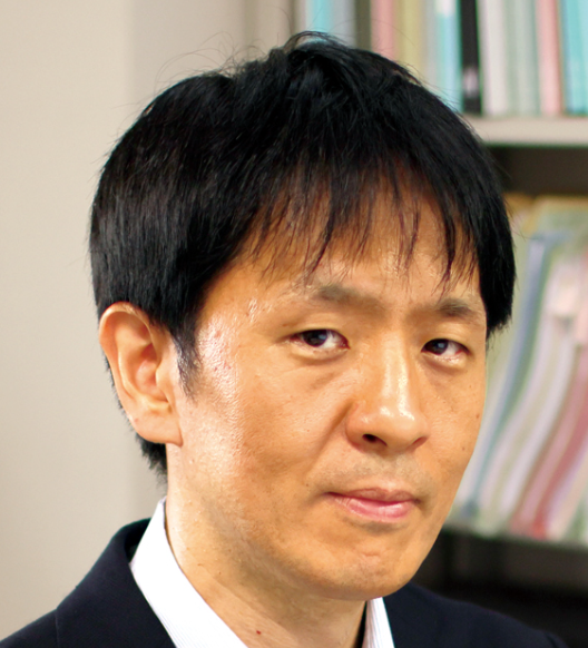 Takeshi Kondo (近藤猛)合作论文数Laser and Synchrotron Research Centre, The Institute for Solid State Physics, The University of Tokyo4
 Ryo Noguchi合作论文数3Masaru Kobayashi合作论文数3
 Kenta Kuroda (黒田健太)合作论文数Department of Physics, Hiroshima University;Graduate School of Advanced Science and Engineering, Hiroshima University;WPI-SKCM23
 Yohei Sato合作论文数3
 Kazunori Ueno (上野和紀)合作论文数Department of Basic Sciences, Graduate School of Arts and Sciences, College of Arts and Sciences, The University of Tokyo3
 Zifan Xu合作论文数Computer Science Department, University of Texas at Austin2Hiroaki Taiko合作论文数2Viktor Kandyba合作论文数2Daehun Lee合作论文数Department of Physics, University of Texas at Austin2Zhanzhi Jiang合作论文数Dept Phys, Univ Texas Austin2Alessio Giampietri合作论文数Elettra Sincrotrone Trieste ScPA2Cédric Bareille合作论文数2Hiromasa Namiki合作论文数2
 Cephise Cacho合作论文数Central Laser Facility, Rutherford Appleton Laboratory;Diamond Light Source2
 Yoshihiro Iwasa (岩佐義宏)合作论文数RIKEN Center for Emergent Matter Science2
 Shuichi Murakami (村上修一)合作论文数Department of Physics, Tokyo Institute of Technology2
 Ryotaro Arita合作论文数Department of Physics;University of Tokyo;Department of Physics, University of Tokyo2Takashi Miyake合作论文数2
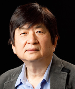 Shik Shin (辛埴)合作论文数Laser and Synchrotron Research Center, Institute for Solid State Physics, Division for Strategic Public Relations, The University of Tokyo2
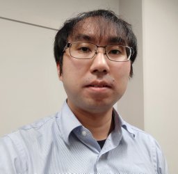 Masayuki Ochi (越智正之)合作论文数Department of Physics, Graduate School of Science, Osaka University2Ayumi Harasawa合作论文数Synchrotron Radiation Laboratory, Institute for Solid State Physics, The University of Tokyo2
 Timur Kim合作论文数Diamond Light Source2
 Koichiro Yaji (矢治光一郎)合作论文数Center for Basic Research on Materials, National Institute for Materials Science;Unprecedented-scale Data Analytics Center, Tohoku University2
 Alexey Barinov合作论文数Elettra-Sincrotrone Trieste S.C.p.A.2
 Yumiko Katayama合作论文数Graduate School of Agriculture, Kyoto University2
 Toshiya Ideue合作论文数2
 Keji Lai合作论文数Department of Physics, College of Natural Sciences, University of Texas at Austin2Chun Lin合作论文数1C. Bareille合作论文数1Murase Masayuki合作论文数1Kifu Kurokawa合作论文数1Mitsuhiro Nakayama合作论文数1So Kunisada合作论文数Univ Tokyo, ISSP, Kashiwa, Chiba 2778581, Japan1Takuya Nakano合作论文数1Hiroaki Tanaka合作论文数Inst Solid State Phys, Univ Tokyo1
 Peng Zhang合作论文数Univ Calif Los Angeles, Dept Elect & Comp Engn, Los Angeles, CA 90095 USA1Shunsuke Sakuragi合作论文数1Rikizo Yano合作论文数Inst Mat & Syst Sustainabil & Appl Phys, Nagoya Univ1Zhang Peng合作论文数1
 Araki Yusuke合作论文数Dept Mat Life Sci, Osaka Univ1
 Masato Sakano (坂野昌人)合作论文数Department of Engineering Science, The University of Electro-Communications1
 Moritz Hoesch合作论文数Deutsches Elektronen-Synchrotron1
 Donghui Lu合作论文数SLAC National Accelerator Laboratory, Stanford University1
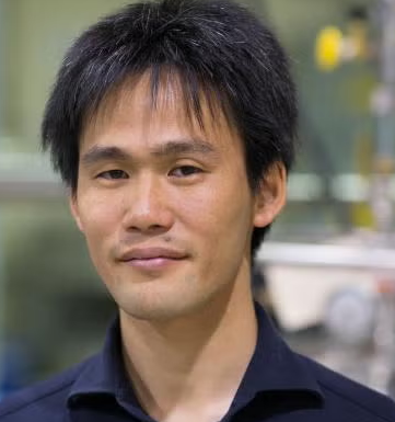 Makoto Hashimoto合作论文数SLAC National Accelerator Laboratory;Stanford Institute for Materials and Energy Sciences, Stanford University1Tetsuroh Shirasawa (白澤徹郎)合作论文数National Metrology Institute of Japan, National Institute of Advanced Industrial Science and Technology1




