A multiplierless processor architecture is proposed for hardware implementation of fast Fourier transform. Distributed arithmetic is applied to simplify expensive butterfly operations and twiddle multiplications. The novel architecture can largely reduce area cost by replacing complex multipliers and adders with DA lookup tables. Both 8-bit and 16-bit 64-point FFT processors were designed, and the synthesis result shows the designs can attain much lower area cost while keeping real-time processing speed.
Here we present a novel 64-bit adder carry chain design implemented in Inverted-Domino (iDomino) logic that is an improved style over conventional Domino for better performance. In the proposed scheme capacitances at output node are reduced and foot transistor in Domino logic is absorbed into clock tree to increase circuit speed. A 64-bit lookahead carry chain is constructed and HSPICE simulation in 0.25um CMOS parameter shows that carry propagation can be done in less than 480ps and a 20% speed enhancement over Domino is achieved.
A 32bit Java-based processor is designed for mobile multimedia applications to run MIPS-compatible local instructions and some application-specific Java bytecodes in a RISC-like architecture. In Java-mode, some Java bytecodes employed in the specific application are decoded into local instructions by VLSI implementation. With VHDL simulation tools, SW/HW co-design verified that Java bytecodes could be executed on the processor with a local thread for a real-time visual processing. Furthermore, the design was synthesized to physical layout according to 1.2 /spl mu/m standard CMOS technology and the simulation shows that the processor can run at a frequency of 20 MHz.
An improved CMOS snapshot readout structure called RRSCA (Reset Row-by-row Snapshot Charge Amplifier) for infrared focal plane array (IRFPA) is presented in this paper. The pixel circuits in RRSCA readout structure are reset row by row after each row's pixel signals were readout to the column stage in parallel and pixel circuit is very simple including only three MOSFETs. Thus, the RRSCA readout structure is very suitable for the readout circuit design with large-format and very small pixel size such as 30*30 or 25*25 μm 2 . An experimental 130 × 130 RRSCA chip has been fabricated with 1.2-μm Double-Poly Double-Metal (DPDM) n-well CMOS technology. Both simulation results and experimental results are presented.
Circuit design of 32-bit Logarithmic Skip Adder (LSA) is introduced to implement high performance, low power addition. At architecture level, ELM carry look ahead adder is included into blocks of carry skip adder and the hybrid architecture of LSA costs 30% less hardware than ELM. At circuit level carry-incorporating structure to include the primary carry input in carry chain and and-xor structure to implement final sum logic are designed. Circuit simulation using spectre simulator are presented and compared with recent literatures'. For 2.5 v, 0.25 /spl mu/m process, critical delay of 0.8 ns, power dissipation of 5.2 mw at 100 MHz is simulated.
 lijiu ji (吉利久)合作论文数3
 Zhongjian Chen (陈中建)合作论文数School of Integrated Circuits, Peking University3liu ling合作论文数2B. Yang合作论文数2
 Jun Gao (高军)合作论文数Institute of Data Science and Engineering, School of Computer Science, Peking University;Key Laboratory of High Confidence Software Technologies, Peking University2
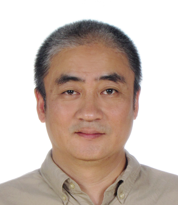 Ming Jiang (姜明)合作论文数Department of Information and Computational Sciences, School of Mathematical Sciences, Peking University2cui wentao合作论文数1Wang Xinan合作论文数1gao jun合作论文数1jing liu合作论文数1S. Jia合作论文数1
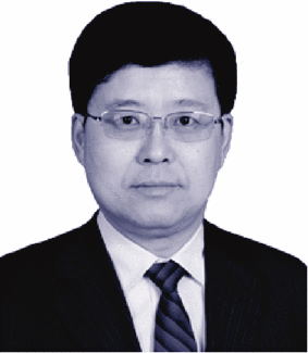 Ju Tang合作论文数1
 Song Jia (贾嵩)合作论文数School of Integrated Circuits, Peking University;School of Electronics Engineering and Computer Science, Peking University1
 Yangyuan Wang (王阳元)合作论文数School of Electronics Engineering and Computer Science, Peking University1
 Ru Huang (黄如)合作论文数Institute for Artificial Intelligence, Peking University1
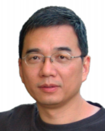 Fei Liu (刘飞)合作论文数School of Internet of Things Engineering, Jiangnan University1Wengao Lu合作论文数1
 Jingzhi Han (韩景智)合作论文数School of Physics, Peking University1




