Wet chemical etching serves as a critical fabrication process for gallium nitride (GaN)-based devices, while precisely measuring the overall etch rates of GaN is essential for both precise control and mechanism research of this process. In this study, the anisotropic etching behavior of Ga-face GaN in 5 wt % KOH/ethylene glycol (EG) solution (110-130 °C) is systematically investigated for the first time. By innovatively designing samples containing micrometer-level hemisphere and wagon-wheel structures, the overall etching rates of Ga-face GaN in the KOH/EG system are experimentally determined accurately. Subsequently, this research compares the etching rate distribution differences between the H3PO4 and KOH/EG systems for Ga-face GaN, and determines the activation energies of arbitrary crystal planes that can be calculated by the overall etching rate distribution in the KOH/EG system at different temperatures (110-130 °C). Furthermore, in this paper, the anisotropic mechanism of the etching rate is established under the assumption of step flow, the etching mechanism is given based on the calculated removal rate of atomic clusters, and the reasons for the etching rate distribution in different etchants are explained on the atomic scale. In addition, in GaN microstructure etching experiments, the evolution of the etching morphology of the hexagonal concave structure is accurately predicted based on the experimentally determined etching rate data of the overall crystal planes. The results of this paper provide critical experimental paths, overall etching rate distribution data, and theoretical support for the precision control of wet etching of GaN micro- and nanostructures.
In particle-in-cell (PIC) simulations, the electromagnetic model requires solving Maxwell’s curl equations while preserving charge conservation since violations of the charge continuity equation inevitably accumulate errors and degrade the result’s fidelity. However, conventional approaches for error mitigation, such as higher order weighting schemes and digital smoothing techniques, often introduce either implementation complexity or prohibitive computational costs. To overcome these limitations, we have developed a physics-informed neural network (PINN) framework for direct field correction. In this article, thestandard Maxwell’s curl equations are solved first. Then, the PINN-based correction is employed to effectively suppress the divergence error. Furthermore, the developed PINN framework is extended to electrostatic simulations through the inherent charge conservation properties embedded in Maxwell’s equations. This advantage eliminates the need for separate electrostatic solvers while maintaining accuracy in capacitively coupled plasma (CCP) discharge simulations, as verified through comprehensive benchmark testing. This unified framework offers significant advantages in both computational efficiency and implementation simplicity compared to traditional correction methods.
The numerical prediction of ablation processes induced by femtosecond lasers is increasingly important for understanding and optimizing laser-material interactions, yet traditional experimental and conventional numerical methods often face limitations-particularly in multi-material problems-due to their high computational cost and reliance on extensive datasets. This work presents a multi-material computational framework for femtosecond laser processing based on physics-informed neural networks (PINNs), which leverage physical laws to eliminate the need for large training datasets while retaining the flexibility of machine learning. The framework predicts the spatial-temporal evolution of free electron density and temperature during femtosecond laser irradiation and employs transfer learning to efficiently adapt to varying processing conditions (e.g., pulse energy, pulse duration) across different materials. It can also perform inverse estimation of process parameters from the observed machining profile. In the model construction, hard constraints are imposed to satisfy the boundary and initial conditions, and the loss function incorporates residual terms derived from the governing equations of free electron density and temperature, rather than conventional data-based loss terms. Validation on various microdevice materials shows that, for borosilicate glass, the predictions from the PINN model are highly consistent with the experimental machining profiles. Furthermore, the transfer learning process significantly accelerates convergence and accurately predicts the distribution of free electron density and temperature for silicon carbide. In inverse modeling, the laser fluence obtained for gallium nitride agrees well with the ablation experimental measurements, confirming the accuracy, efficiency, and applicability of this framework in addressing laser-matter interaction problems across multiple materials.
Focused helium ion beam allow for precise processing of materials on the nanoscale, but inevitably causes damage to the substrate. Therefore, developing a damage model is essential. The damage caused by helium ions to the substrate primarily includes the amorphization damage to the crystalline materials and helium bubble formation due to helium accumulation inside the material. In this paper, a helium bubble damage model is proposed which utilizes the population balance equation to solve for the helium bubble distribution, enabling simulation of helium bubble growth and aggregation within the substrate under specific ion energies and doses. Simultaneously, silicon was subjected to focused helium ion beam implantation, followed by sample preparation and observation using Transmission Electron Microscopy (TEM). Finally, the simulation results were compared with the experimental observations to verify the accuracy of the model.
We developed a traditional computational framework coupling time-dependent external circuit equations with a 2D3V axisymmetric Particle-in-Cell/Monte Carlo (PIC/MC) model. By solving circuit equations at each time step, this framework establishes bidirectional feedback between plasma dynamics and self-bias voltage evolution. Moreover, the superposition of Laplace and Poisson solutions is introduced to avoid solving iteratively for the potential on the boundary, which demands extra Laplace solvers for the direct implicit scheme. To improve computational efficiency, a generative network, named Conditional Variational Autoencoder (CVAE), is implemented to predict self-bias voltage effects, achieving a remarkable 25,000x acceleration compared to the circuit solver while maintaining > 90% waveform fidelity. The grid-independent nature of the CVAE architecture enables parametric studies with arbitrary resolution and reverse-optimization targeting desired self-bias voltages and currents. Furthermore, a novel hybrid framework combining the PIC/MC model with the CVAE surrogate is proposed to enhance computational efficiency in plasma simulations. Numerical simulations of voltage-driven CCPs under varied gap conditions demonstrate the hybrid PIC/MC-CVAE model's capability to quantify self-bias effects, revealing their dependence on electrode configurations. This methodology successfully bridges plasma kinetics and macroscopic circuit behavior, providing an efficient and robust tool for optimizing CCP-based industrial processes.
To comprehensively investigate the evolution of the stress field, a three-dimensional thermodynamic model of laser cladding was developed in this paper. By analyzing the physical process and constructing a mathematical model, the temperature transfer and stress distribution were calculated. The simulation examined the evolution and distribution of stress at various scanning speeds, discussing the interplay between the temperature field and the stress field during rapid heating and cooling. Residual stress was measured through X-ray diffraction in experiments, and the crack distribution within the cladding layer was observed. The findings indicated that the stress values calculated from the simulation model aligned well with the experimental results. By combining experimental data, we conducted a qualitative analysis of the distribution of residual stresses and the trends of crack initiation, leading to the proposal of an optimized processing scheme that significantly enhances the quality and reliability of the cladding layer.
This study introduces a follow-control method for lower limb rehabilitation robots, leveraging model predictive control (MPC) and a Fiducial Marker system. As stroke incidence rises, leading to significant motor dysfunction, effective rehabilitation techniques have become crucial. The proposed method employs ARTag markers to accurately capture target positioning and posture information, while MPC ensures precise follow-control of the robotic system. Experimental validation confirms that this control strategy effectively maintains tracking accuracy within predefined error constraints, providing a safe and comfortable rehabilitation experience for patients. This approach underscores the potential of rehabilitation robots to improve recovery outcomes for individuals with lower limb impairments.
This study presents an in-depth analysis of substrate lattice disorder in GaN and AlN, particularly GaN, under controlled precise irradiation achieved by helium ion microscopy. GaN was exposed to various irradiation fluences (0.01-0.1 nC/mu m) at beam energies of 15 key and 35 key, with subsequent lattice disorder characterized using scanning, high resolution transmission electron microscopy, and energy dispersive spectroscopy. The results reveal that the defective region in GaN is characterized as a vase-shaped profile comprising a bulbous region filled with helium bubbles attached to dislocation loops and a locally amorphous neck region. As the irradiation fluence increases or the beam energy decreases, the defects become denser, leading to the formation of complex defective structures and severe lattice distortions. Under irradiation condition of 15 key paired with 0.1 nC/mu m, crystallographic misorientation, surface swelling, nanocracks formed by the lateral coalescence of helium bubbles, the deficit of N atoms and enriched Ga nanocrystals are identified. The AlN substrate exposed to irradiation exhibits similar damage profiles to GaN, but there is no preferential disordering of the AlN surface. This study enhances the understanding of ion-induced lattice disorder in III-nitrides under light gas ion implantation, providing valuable insights into the irradiation response of III-nitrides.
Currently, the time and cost required to obtain large datasets limit the application of data-driven machine learning in nanoscale manufacturing. Here, we focus on predicting the nanoscale damage induced by helium focused ion beams (He-FIBs) on silicon substrates. We briefly review the most relevant atomistic defects and the partial differential equations (PDEs), or rate equations, that describe the mutual creation and annihilation of the defects, eventually leading to the amorphization of the substrate and, the nucleation and early growth of helium bubbles. The novelty comes from the use of a physics-informed neural network (PINN) to simulate quantitatively the evolution of the bubbles, thus bypassing the dataset availability problem. As usual, the proposed PINN learns the underlying physics through the incorporation of the residuals of the PDEs and corresponding Initial Conditions (ICs) and Boundary Conditions (BCs) in the network's loss function. Meanwhile, the system of PDEs poses some challenges to the PINN modeling strategy. We find that (i) hard constraints need to be imposed on the network output in order to satisfy both BCs and ICs, (ii) all the inputs and outputs of the PINN need to be cautiously normalized to ensure convergence during training, and (iii) customized weights need to be carefully applied to all the PDE loss terms in order to balance their contributions, thus improving the accuracy of the PINN predictions. Once trained, the network achieves good prediction accuracy over the entire space-time domain for various ion beam energies and doses. Comparisons are provided against previous experiments and traditional numerical simulations, which are also implemented in this study using the Finite Difference Method (FDM). While the L2 relative errors for all collocated points remain below 10%, the accuracy of the PINN decreases at lower beam energies and larger ion doses, due to the presence of higher numerical gradients.
In order to study the profile formation of photoresist microstructure (such as microlens) by the thermal reflow method, the viscoelastic dynamic model is developed based on motion equation, continuity equation, and thin film assumptions. The influence of viscoelastic properties, surface tension, as well as crosslinking effect on polymer melt profile evolution, are considered in this model, and the Oldroyd-B model is used to describe the viscoelastic constitutive relation of polymer melt. Since the viscoelastic dynamic model developed in this paper is a differential equation with regard to the height function of the polymer melt profile, the free surface profile of polymer melts can be obtained naturally during shape evolution by numerically coupling the solution of the film thickness equation and the Oldroyd-B constitutive equation. The computational efficiency of numerical simulation of the free-surface profile would be improved by using this equation as compared to solving the highly non-linear equations of viscoelastic hydrodynamics. The influence of key parameters such as baking time, baking temperature, and crosslinking effect on profile shape evolution is analyzed by this model, and the materials are compared by assigning them different Weissenberg number. In addition, the maximum relative error of verification experiments between the final profile predicted by the simulation and the experimental results is less than 10 %.
In the developed particle-in-cell/Monte Carlo collision (PIC/MCC) model, the iterative solution of Poisson's equation dominates computational resource consumption, while parallelization has optimized other components. To reduce these costs, neural networks are introduced for accelerating field solvers. However, direct solutions by neural networks exhibit significant performance degradation under noisy conditions, which requires increased particle counts and substantially increases particle-pushing runtime. To overcome this limitation, we propose physics-informed neural networks (PINNs) for estimating initial conditions and use iterative solutions for smoothing noise. Furthermore, a novel hybrid method that integrates PINNs with multigrid methods is developed, achieving accelerated convergence and enhanced computational efficiency. Benchmark test results are then presented to validate both the Poisson solver and the integrated PIC/MCC framework. These results advance plasma physics research, thus providing guidance for plasma source design aimed at process optimization.
With the development of micro-nano-scale devices, the precise manufacturing of complex topographies using focused ion beam (FIB) sputter etching has become an indispensable process requirement. The fabrication of curved micro-nano structures primarily employs bitmaps and stream files. However, due to the influence of complex effects, it is challenging to directly ascertain the process parameters. Therefore, this paper intensively analyzes the FIB manufacturing method, focusing specifically on the control methodology of bitmaps and stream files in the production of complex structures. Furthermore, the multi-strategy optimization model based on CCAPSO (Continuous Cellular Automaton & Particle Swarm Optimization) is proposed, integrating simulation and optimization techniques to acquire process parameters and enhance manufacturing accuracy. The model leverages the characteristics of FIB sputter etching, simplifying the solution space, optimizing the search method, and increasing the iteration rate. Additionally, various complex structure manufacturing experiments were designed to validate the model's effectiveness and rationality. The advantages and limitations of the optimization methods and the three strategies are elaborated in detail, and their application in real manufacturing scenarios is also discussed, providing a reference for the further application of FIB manufacturing technology.
beta - Gallium oxide (beta - Ga2O3) is an ultra-wide bandgap (UWBG) semiconductor that is widely recognized as an ideal material for the fabrication of optoelectronic and high-voltage devices. As an advanced sputtering etching technology, focused ion beam (FIB) is increasingly used in the micron and nanoscale processing of semiconductor materials. In this paper, the influence of Ga FIB on /1 - Ga2O3 sputtering etching is systematically investigated from three parts, namely, the calibration of sputtering yield, the influence of process parameters on etched profiles and the effect of redeposition. Firstly, sputtering etching of /1 - Ga2O3 substrate was carried out under typical processing conditions with different incident angles, and the key parameter of sputtering yield was precisely calibrated. Further, Yamamura's model is applied to fit the curve of sputtering yield as a function of incident angle. In addition, the sputtering yield of /1 - Ga2O3 is compared with those of GaN and Si under the same conditions, revealing the differences between them. Next, through line scan etching and trench structure etching experiments, this study analyzed the maximum etched depth, width, and etched volume variation with ion dose. The evolution of /1 -Ga2O3 trench structure is described and compared with GaN and GaAs, and from the perspective of redeposition effects, the reasons for the differences between the three in the sputtering etching process are analyzed. Lastly, the study investigated the impact of FIB process parameters on the redeposition effects of /1 - Ga2O3. Experimental results indicated that significant redeposition effect occurs when etching /1 -Ga2O3 with large single dwell time. Further analysis identified a specific range of single dwell times under different beam currents that reduce redeposition and prevents the formation of sidewall angles. These findings provide important data support for the high-resolution etching process of /1 - Ga2O3-based micro-nano devices using FIB technology, and also establish a reliable data foundation for related simulation studies.
The research designs a novel micrometer-level hemisphere structure and develops a focused ion beam process to fabricate the high-precision microsphere samples. The experiment successfully determines the overall distribution of the etch rate of Ga-face GaN in an anisotropic etchant for the first time. Subsequently, based on the level set method, an etching process model supporting a combined focused ion beam and wet etching process for GaN is established, successfully simulating the entire etching process of nanowire arrays.
The Ga-face gallium nitride (GaN) crystal has recently attracted significant research interest in the micro/nano device due to its exceptional properties. Therefore, exploring low-cost and high-efficiency anisotropic wet etching processes for GaN material is essential. This research investigates the measurement of the overall anisotropic etching rates by introducing a novel micrometer-level hemispherical structure. For the first time, we report the full anisotropic etching rate distribution for Ga-face GaN crystal planes based on the etched results of the micro hemisphere and wagon-wheel structure specimen. The etching experiments were carried out in 85 %wt H 3 PO 4 etchant at 130 degrees C and 150 degrees C. The etching result of Ga-face GaN crystal orientations displays a hexagonal symmetry pattern. In addition, the overall etch rates measurement enables the identification of the crystal planes with maximum and minimum etch rates at different temperatures, and the experiment also shows the etch rate of primary crystallographic orientations, such as +c-plane, m-plane, and a-plane. Finally, the atomic structures of GaN crystallographic planes are analyzed to explain the anisotropy in the etching process on different crystal zones by the step-flow mechanism. The resulting etch rate database allows the numerical simulation of the etch front and helps understand the etching mechanism of the GaN crystal.
The thermal behavior of the cladding layer and the flow behavior of the molten pool significantly affect the geometry, temperature distribution and microstructure of the cladding track, thus affecting the mechanical properties of the cladding. Based on the interaction between the laser and powders, a calculation method of the cross-sectional area of the cladding track is proposed. The droplet energy method and the moving grid method are first combined to establish the surface growth model of the cladding track, to calculate the geometry of the cladding track. Then, the temperature field and flow field of the cladding track are studied. The driving forces of the molten pool flow including shear viscosity, gravity, buoyancy, surface tension at the gas-liquid boundary and pressure between liquids are considered to carry out the dynamics study of the molten pool. According to the force condition of the infinitesimal in the molten pool, the dynamic rules and boundary rules of the molten pool are established, so as to solve the flow field of the molten pool. In addition, the calculated geometry of the cladding track is compared with the experimental result to verify the accuracy of the model, and the microhardness of the cladding track is measured. The results show that the relative error between the simulation and the experiment is less than 6%, and the microhardness of the cladding layer is significantly improved. This work can provide a method for studying the morphology, temperature field, and flow field of laser cladding.
In this paper, a combined transport-defect evolution multiscale model describing the generation and the evolution of microstructure damage in silicon carbide (SiC) induced by focused helium ion beams is developed. In the proposed model, the transport of helium ions and displaced atoms in the SiC substrate and the generation of point defects are described by the Boltzmann transport equations, while the subsequent defect evolution is characterized by a set of rate equations with the contributions of the modeling of the bubble coalescence as well as the substrate swelling. The validity and superiority of the transport equations are verified by comparing the simulation results with the data from experimental measurements and available simulation methods. The subsurface amorphous profile, onsurface swelling profile, and the spatial and size distribution of helium bubbles in a SiC substrate irradiated by focused helium ion beams are simulated using the proposed multiscale model. The damage morphology simulated by the proposed model is in good agreement with the transmission electron microscopy images at different beam energies and doses. This work provides an effective tool for full-stage modeling of complex evolutionary mechanisms of microstructure damage induced by precise and high-throughput helium irradiation.
Silicon carbide is receiving increasing attention as a substrate due to its stability in harsh environments. At the same time, further minimization of sensors and micro devices requires new techniques for nanofabrication. In this context, the helium focused ion beam (He-FIB) is a promising candidate, due to its high resolution and capability of sub-10 nm fabrication, as well as its ability to modify the properties of the substrate via ion implantation. In this work, we consider previously reported experimental images of subsurface damage in both SiC and Si, as induced by He-FIB under line scanning, and provide a summary of the resulting amorphous and bubble regions as a function of the beam energy and dose. Based on empirical relations collectively encapsulated into a damage profile function (DPF) that was previously used to describe the contour of the amorphous region in Si, we focus on presenting a generalized damage profile function (GDPF) that enables describing the contours of both the amorphous and bubble regions in SiC simultaneously. In particular, the role of swelling, as a relatively small protruding region from the initial surface that eventually restricts the upward expansion of the bubble region, is fully considered. The parameters of the resulting mathematical model are related to measurements from the experimental cross-sectional images and are eventually optimized by using an evolutionary algorithm. Comparison to the experimental profiles concludes that the proposed GDPF captures both the amorphous and bubble region profiles with good precision.
 Wencheng Tang (汤文成)合作论文数School of Mechanical Engineering, Southeast University39
 M. Gosalvez合作论文数Department of Oncology, Hospital General de Asturias36
 Xiaoli Qiu (仇晓黎)合作论文数School of Mechanical Engineering, Southeast University23
 Zaifa Zhou (周再发)合作论文数School of Integrated Circuits, Southeast University23
 Kazuo Sato合作论文数Research Institute for Industrial Technology, Aichi Institute of Technology22
 Qing Chai (柴青)合作论文数21
 Hong Yi (易红)合作论文数School of Mechanical Engineering, Southeast University20
 Chen Fang合作论文数18
 Qianhuang Chen合作论文数14
 Prem Pal合作论文数National Physical Laboratory;Centre for Applied Research in Electronics;Indian Institute of Technology;Centre for Applied Research in Electronics, Indian Institute of Technology14
 Yuan Li合作论文数13XiaoLi Chou (仇晓黎)合作论文数13Chen Ye合作论文数12
 Jun Ni (倪军)合作论文数Global Institute of Future Technology, Shanghai Jiao Tong University;S.M. Wu Manufacturing Research Center, Department of Mechanical Engineering, University of Michigan12Minghui Pan合作论文数10
 Hui Zhang (张辉)合作论文数School of Energy and Environment, Southeast University10
 Xiaohui Lin (林晓辉)合作论文数School of Mechanical Engineering, Southeast University9
 Guorong Wu合作论文数8
 Zhonghua Ni (倪中华)合作论文数School of Mechanical Engineering, Southeast University8Xi Lin合作论文数6hong yi (易红)合作论文数5
 Huachen Peng合作论文数5
 Chibin Zhang (张赤斌)合作论文数School of Mechanical Engineering, Southeast University5Xin Zhou合作论文数4Junyang Hu (胡钧阳)合作论文数4Penghao Dong合作论文数Department of Mechanical Engineering, Stony Brook University4Xianqiang Cheng合作论文数4Tianyang Shao合作论文数4
 Haoyang Liu合作论文数4
 H. Hida合作论文数3Xinyan Guo合作论文数3Zhiyue Guo合作论文数3Yunze Zhang合作论文数3Dongliang Huang合作论文数3Sajal Singh合作论文数3
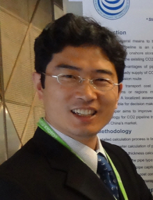 Qi Li (李琦)合作论文数University of Chinese Academy of Sciences;Institute of Rock and Soil Mechanics, Chinese Academy of Sciences3
 Risto Nieminen合作论文数Department of Applied Physics, Aalto University3
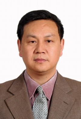 Wenhe Liao (廖文和)合作论文数School of Mechanical Engineering, Nanjing University of Science & Technology;College of Mechanical Electrical Engineering, Nanjing University of Aeronautics and Astronautics3
 Ye Chen (陈烨)合作论文数School of Architecture, Southeast University3Siyuan Sun合作论文数2Jiabao Yao合作论文数2Yuchao Li合作论文数2Jin Qian合作论文数2Jun NI (倪俊)合作论文数2Peng Zhu合作论文数2
 Subhomoy Haldar合作论文数NanoLund and Solid State Physics, Lund University2jinping xiao (肖金平)合作论文数2WeiJun Tang (唐维俊)合作论文数2KeCun Ben (贲可存)合作论文数2




