A novel LC bandpass filter (BPF) is proposed, in which its resonator is constructed solely by a novel active inductor (AI) instead of physical L and C components. The novel AI is composed of Gm-boosted Dual-parallel positive transconductor, Gm-boosted Dual-parallel negative transconductor, modulation cell, and transconductor noise suppression branch to simultaneously achieve high quality factor (QL), wide-range tuning of both inductance values and resonant frequencies, and low noise. Furthermore, taking full advantage of the fact that the novel AI can be equivalent to a parallel R-L-C network, the passive inductor L and capacitor C in the traditional BPF are replaced by the single novel AIto function as the resonant components, and thus the novel AI-based BPF topology is constructed along with a low-noise differential input stage and a negative-resistance generation circuit. The collaboration among these building modules enables the BPF to achieve better overall performance in terms of high reconfigurability of center-frequency, compact area, high quality factor (QBPF), and low noise. The novel BPF is laid out and verified by post-layout simulation in a 180 nm CMOS process. The results show that the BPF achieves a compact layout area of 44.8 mu m & times; 35.6 mu m, a wide tuning range of center frequency from 1.3 GHz to 4.63 GHz, a minimum noise figure of 14.4 dB, and a maximum QBPF of 35. The architecture of this proposed BPF provides a new solution to the design of a high overall performance BPF.
A top-illuminated GaN/InGaN avalanche heterojunction phototransistor (AHPT) based on heterojunction amplification and avalanche multiplication was proposed to overcome limitations in responsivity and sensitivity of GaN/InGaN detectors for ultraviolet (UV) detection. The top-illuminated structure was designed to enhance the current gain and response speed in HPT mode, ensure the breakdown voltage and carrier multiplication efficiency in APD mode, and meanwhile expand the spectrum bandwidth of the response. Based on a developed analytical model, the electric field distribution, energy band characteristics, and optoelectronic performance of the top-illuminated GaN/InGaN AHPT were analyzed when the phototransistor operated in HPT, APD, and AHPT modes, respectively. The simulation results demonstrate that the top-illuminated GaN/InGaN AHPT achieves a peak responsivity of 1.3 A/W in HPT mode, a responsivity of 4.0 A/W in AHPT mode, and a responsivity exceeding 100 A/W in APD mode due to avalanche multiplication. The dark current remains at 10(-7)A and the maximum specific detectivity achieves 8 & times; 10(12) cm & centerdot; Hz(0.5) & centerdot; W-1. The 3-dB bandwidth increased from 50 MHz in HPT mode to 200 MHz in APD mode, achieving an excellent balance between response speed and gain. In AHPT mode, the top-illuminated structure extended the spectral response to a wider band range of 350-418 nm, significantly improving UV detection capabilities.
This paper presents an adjoint-sensitivity-assisted surrogate optimization technique for high-power microwave filters. In multiphysics (MP) filter design, direct MP optimization is computationally expensive and may converge poorly when the starting point is far from the specifications. Existing feature-assisted surrogate optimization reduces this difficulty by using low-dimensional response features, but a surrogate trained only with feature values may still require repeated MP evaluations. The presented technique incorporates both MP response sensitivities and adjoint feature sensitivities into the surrogate training. A scale-balanced objective function is also used to combine response constraints and feature terms during trust-region optimization. A high-power waveguide filter example is used to validate the feasibility of the technique.
As microwave devices evolve toward miniaturization and high-power operation, multiphysics (MP) simulation becomes essential to accurately capture real-world performance. However, MP-based optimization is more challenging than pure electromagnetic (EM) optimization due to its high computational cost, and the direct MP optimization process is easy to become trapped in local minima when the initial design is poor. While feature-assisted surrogate optimization has proven effective in solving this issue, its efficiency can be further improved. This letter proposes a novel sensitivity-based feature-assisted MP surrogate optimization technique. For the first time, adjoint sensitivity information is incorporated into the training of the MP-based feature surrogate, which significantly enhances sample efficiency and model accuracy. Furthermore, a scale-balanced objective function is formulated to eliminate dimensional disparities and accelerate convergence. The effectiveness of the proposed technique is validated through two microwave filter design examples.
Neuro-transfer function (Neuro-TF) has emerged as a prominent approach for electromagnetic (EM) parametric modeling, though traditional implementations for TF parameter extraction relying on vector fitting often suffer from parameter discontinuity. In this letter, we propose a novel framework integrating 1-D convolutional autoencoder (1D-CAE) with adjoint sensitivity analysis to establish high-fidelity parametric models for microwave filters. The proposed 1D-CAE-based TF parameter extraction captures intricate frequency-dependent relationships within S-parameters through its hierarchical convolutional layers, achieving efficient dimensionality reduction while preserving essential EM characteristics. To accelerate the training process, an adjoint sensitivity-enhanced multilayer perceptron (MLP) and EM sensitivity are used to map geometric parameters to the extracted TF parameters. The final hybrid architecture combines the sensitivity-informed MLP with the 1D-CAE decoder to form an end-to-end surrogate that directly translates geometric parameters into EM responses. Compared to conventional neuro-TF approaches, the proposed method achieves better model accuracy with fewer TF parameters. Two microwave filter modeling examples are provided for demonstration.
Silicon-based phototransistor detectors, offering advantages such as high internal gain, cost-effective and compatibility with CMOS technology, are becoming one of the key devices for large-scale photon integration chip and have significant potential for applications in short-distance optical interconnecting. To relieve its inherent optimization contradiction between responsivity and bandwidth performance, a novel couple ridge waveguide SiGe/Si phototransistor was proposed, in which the carrier transport and the photon propagation were perpendicu & hybull; lar and demonstrate the independent optimization on absorption efficiency and operating speed. The optical propa & hybull; gation mode in the SiGe/Si ridge waveguide were analyzed between the single mode and the multiple mode. The geometric parameters of the ridge waveguide to achieve high absorption efficiency were optimized. The ridge waveguide SiGe/Si phototransistor were fabricated using technology compatible with CMOS process platform and achieved a responsivity of 6. 4 A/W with the dark current of 10 nA.
This paper presents a dynamic orthogonal sampling method to improve the efficiency of automated model generation (AMG) for high-dimensional microwave filters. The method integrates dynamic sampling with orthogonal Design of Experiments (DoE). It begins with an initial orthogonal sample set and iteratively refines sampling in nonlinear regions through local interpolation while preserving data orthogonality. Compared with existing grid-based sampling approaches, the orthogonal sampling method significantly reduces data requirements and computational cost while maintaining modeling accuracy. The modeling results demonstrate its effectiveness for efficient high-dimensional microwave modeling.
This paper proposes a novel band reject filter (BRF) composed of a high-performance active inductor (AI), an active capacitor module (ACM), a negative active capacitor module (NACM), a biasing module and input/output stages. The AI, built with dual gyrators, an RC feedback branch, a feedforward noise-suppression circuit, and two tunable current sources, achieves enhanced quality factor $(Q_{\mathrm{L}})$, low noise, and wide inductance tuning range. Furthermore, the AI and ACM are employed to replace passive $L$ and $C$ in conventional BRFs to form a series $L C$ resonator, which is then combined with NACM, biasing module and input/output stages to construct the complete BRF. Consequently, the BRF achieves a compact area, low noise, highly reconfigurable center frequency, and deep notch rejection. Fabricated in a TSMC $0.18 \mu \mathrm{m}$ CMOS process, the BRF occupies a layout area of only $1159.2 \mu \mathrm{m}^{2}$, features a center frequency tunable from 2.47 to 5.35 GHz, a low passband noise ranging from 4.1 to 6.9 dB, and a minimum notch depth of −28 dB.
Silicon-based heterojunction phototransistors (HPTs) have attracted considerable interest for high-sensitivity photodetection owing to their high current gain and low noise. In order to optimize its trade-off between optical responsivity and operation speed, this work proposes a SiGe/Si HPT integrated with a square-lattice periodic nanohole (NH) array. The matching conditions for coupling an incident plane wave into the different Bloch modes excited in a SiGe/Si NH array are investigated over the 400-1000 nm wavelength range. Compared to bulk SiGe/Si material, the square-lattice NH array shows significantly enhanced absorption efficiency when coupled into a lateral transmission mode, particularly at longer wavelengths. With a NH array period of 1000nm, the responsivity of the novel integrated device reaches 1.02 A/W under 850 nm, representing an increase of 59.3% over the standard SiGe/Si HPT with the same epitaxial structure and fabrication process. The maximum specific detectivity reaches 4.26 & times; 10(10) cm & centerdot;Hz(0.5)& centerdot;W-1. Furthermore, the proposed phototransistor achieves an optical 3 dB bandwidth of 902 MHz at 850 nm, enabling high-speed operation performance close to that of its conventional counterpart.
This letter proposes an advanced inverse modeling method that combines the neural space mapping (NSM) inverse modeling method with vector fitting (VF) based dimensionality reduction technique. Using vector fitting and its pole-residue decomposition technique, the high-dimensional S-parameters are transformed into a low-dimensional pole-residue physical feature, ensuring physical interpretability while reducing dimensionality. Specifically, we design a novel inverse model structure and a two-stage model training algorithm. It effectively reduces the input dimensionality and the volume of fine data, thereby decreasing computational costs and shortening modeling time. The feasibility of the proposed method is demonstrated through two microwave filter design examples.
A concurrent dual-band low-noise amplifier (DB-LNA) based on active inductors was designed to operate at 2.4 GHz and 5.2 GHz to meet IEEE 802.11 n standards. The conventional common source cascode topology without the source degeneration inductor is implemented in the gain control stage. Input impedance matching is achieved with a single-path circuit resonating at two distinct frequencies, while output matching is accomplished using band-pass and band-stop filters. Active inductors replace traditional passive inductors to reduce layout area, and their high Q factor minimizes power consumption. Furthermore, gate noise is suppressed with a capacitor between source and gate in the input stage. The results show that the proposed DB-LNA has gains of 17.2 dB and 12.0 dB at 2.4 GHz and 5.2 GHz, respectively, with noise figures of 3.5 dB and 4.7 dB. The S-11 and S-22 of the DB-LNA are both less than -10 dB at both frequency bands. The 1 dB compression points are -23.9 dBm at 2.4 GHz and -18.7 dBm at 5.2 GHz, with third-order input intercept point values of -13.1 dBm and -8.3 dBm, respectively. The total power dissipation is 15.72 mW with a 1.2 V supply, and the layout area is 0.32 mm(2).
Automated Model Generation (AMG) algorithms are an important technique for creating Artificial Neural Network (ANN) models in microwave design automation. AMG integrates all the subtasks in ANN development into a unified automated algorithm. The assessments of the ANN training phenomena related to under-learning, over-learning and good-learning are automated and the quantitative links between the accuracy of the ANN model, the amount/distribution of training/testing data, and the size of the neural network are established. In this way, the AMG algorithm automatically creates an ANN model with user-desired accuracy, significantly reducing the human time required for modeling. This paper introduces the state of the art in AMG algorithms and its applications in microwave modeling.
This paper presents an inverse modeling technique for microwave filter using neural space mapping (NSM). By introducing the NSM approach, the amount of data required for inverse modeling training is reduced. Additionally, the input dimension of the inverse model is decreased through the Fourier transform and its low-frequency subspace algorithm. The paper also presents a two-stage training algorithm for the NSM-based inverse model based and its application method in microwave filter design. Compared with direct inverse modeling, this technique can effectively cut down the modeling cost. A microwave filter design example is provided to validate the feasibility of this technique.
Silicon-based hetero-junction phototransistor (HPT) is a potential optical detector promising for communication links in optic-interconnect network due to their advantages of low cost, high internal gain, high sensitivity, and compatibility with CMOS processes. In this work, a SiGe/Si HPT with double-zone base is designed and optimized to provide high responsivity and outstanding frequency characteristics simultaneously. The SiGe HPTs with different window positions and areas are fabricated using BiCMOS-compatible mesa process, and the influence of transverse parameters on HPT performance is analyzed comprehensively. With this design, a maximum optical responsivity of 8.52 A/W and a maximum optical 3 dB bandwidth of 638 MHz are demonstrated. The responsivity bandwidth product achieves 4.69 GHz & sdot;A/W with 50 x 50 mu m(2) optical window on emitter mesa under 850 nm incident light, which is expected to be applied in silicon-based optical connecting technology to simplify the optical receiving circuits and lower its power consumption.
Automated model generation (AMG) algorithms have become popular techniques for the systematic development of artificial neural network (ANN) models for microwave components. However, existing AMG algorithms rely on a grid-based sampling strategy, which can be time-consuming and inefficient for high-dimensional microwave modeling problems. To address this challenge, we propose a novel adaptive orthogonal sampling method for AMG. Starting from a small amount of training data in orthogonal distribution, the proposed method employs stage-wise orthogonal sampling. At each stage, we propose to use interpolation techniques to evaluate the sufficiency of training data and dynamically determine the additional training samples required, as well as their optimal locations within the modeling region. The resulting sampling distribution is efficient, with more samples orthogonally distributed in nonlinear subregions and fewer in smooth subregions. This proposed orthogonal sampling method allows the AMG to use significantly fewer samples than traditional grid-based AMG, effectively improving the efficiency of ANN modeling for microwave applications. Two microwave filter modeling examples are provided for demonstration.
An improved gyrator-capacitor (GC) architecture of active inductor (AI) is proposed, which consists of a dualloop configuration, mainly including a negative feedback loop (NFL) and a positive feedback loop (PFL) and hence is denoted as positive-negative-feedback-GC (PNF-GC). The in-depth cooperation of above dual-loop configuration in conjunction with the dynamically and synergistically tuning of external voltages in different building modules ensure high Q values under low-frequency range and alleviate the degradation impact of the parallel conductance Gp on Q values under high-frequency range, and thereby the proposed PNF-GC architecture can make a single AI achieve high Q values under various radio-frequency bands. Subsequently, based on the TSMC's 0.18-mu m CMOS process, a prototype circuit of AI based on PNF-GC architecture as an exemplary example and its layout are given, so as to demonstrate the performance under quad bands including X, C, S and L bands. The results from post-layout simulation indicate that within the frequency range of the X-band (8-12 GHz), the Q values are all higher than 20, with a maximum Q value of 1068 at 10.2 GHz; within the C-band (4-8 GHz), the all Q values exceed 50 and the maximum Q value reaches 1006 at 6 GHz; within the S-band (2-4 GHz), the all Q values surpass 250, with a peak Q value of 1033 at 3 GHz; and within the L-band (1-2 GHz), the Q values are all higher than 590 and a peak Q value of 1026 appears at 1.5 GHz. The above proposed PNF-GC architecture of AI, which makes a single AI have an ability to obtain high Q within a wide frequency range, is of important significance to frequency reconfigurability of miniaturized RFICs.
This paper presents an operational amplifier(opamp) with an improved recursive folding cascode structure featuring a regulated resistor (RIRFC) at the input stage, a floating current source controlled Class AB structure at the output stage, and Miller capacitors and zeroing resistors bridging the input and output stages. Additionally, chopping units are embedded in both the input and output stages. The cooperative operation of these modules enables the circuit to achieve high gain, wide bandwidth, high stability, and low noise performance. Simulation results based on a $0.18 \mu \mathrm{~m}$ CMOS process show that the operational amplifier has a gain of up to 128.4 dB at low frequencies, a gain-bandwidth product of $\mathbf{4 0. 2 5 ~ M H z}$, a slew rate of $11.62 \mathrm{MV} / \mathrm{s}$, an equivalent input noise of $11.94 \mathrm{nV} / \sqrt{\mathrm{Hz}}$ at 100 Hz, as well as a high power supply rejection ratio and good common-mode rejection ratio.
With the aid of the particle swarm optimization algorithm (PSOA), the layout of 10x10 vertical cavity surface emitting laser (VCSEL) array is optimized to improve the output optical power. The simulation results show that, for the optimized VCSEL array with PSOA, the peak junction temperature is lowered by 6.55K, and the non-uniformity of the junction temperature distribution is improved by 32.56% when compared with the conventional VCSEL array without PSOA. As a result, the output optical power is increased by 89.86%. Furthermore, both the VCSEL arrays with and without PSOA are fabricated and the experimental results are consistent well with the simulation results.
Automated model generation (AMG) is a robust algorithm designed to expedite the development of artificial neural network (ANN) models, particularly widely applied in microwave modeling. AMG algorithm encompasses two key aspects, i.e., data sampling and model structure adaptation. The model structure adaptation process in traditional AMG approaches can only independently adjust the number of hidden layers or the quantity of neurons within these layers, lacking the capability to simultaneously adapt both. To enhance the efficiency of ANN modeling, we present an efficient AMG algorithm utilizing batch-adjustment technique for adaptive ANN structure modification. This algorithm dynamically adds or removes hidden layers in batches, to maintain a balance between the number of layers and neurons. In comparison to traditional AMG algorithms, the ANN structure adaptation of the AMG using the batch-adjustment algorithm is more flexible and the automated modeling process of microwave components is more efficient. This presented AMG algorithm is suitable for neural network modeling of various microwave components, such as microwave filters. The modeling of an iris-coupled cavity filter is used as an example to demonstrate the superior performance of the AMG with the batch-adjustment algorithm.
This letter proposes an advanced automated model generation (AMG) of microwave components using an adjoint artificial neural network (ANN) and electromagnetic (EM) sensitivity analysis. EM sensitivities are integrated into the AMG process for the first time to speed up the automated ANN model development. We propose a novel adaptive sampling algorithm, combining EM sensitivities and interpolation techniques to dynamically determine the optimal sampling scheme. This ensures obtaining the most accurate ANN with minimal data. We also propose a new adjoint ANN training method with EM sensitivities to automatically determine the suitable ANN structure. By utilizing both EM data and EM sensitivities, the modeling efficiency of the proposed AMG is effectively improved compared to existing AMGs. Two microwave modeling examples are provided to demonstrate the proposed algorithm.
 Hongyun Xie (谢红云)合作论文数Information Department, Beijing University of Technology202
 Dongyue Jin (金冬月)合作论文数Information Department, Beijing University of Technology171
 Weicong Na (那伟聪)合作论文数College of Microelectronics, Faculty of Information Technology, Beijing University of Technology56
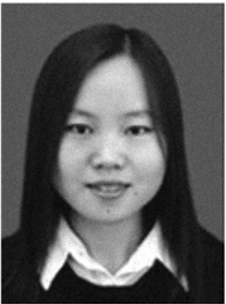 Pei Shen合作论文数53
 Chunbao Ding合作论文数40
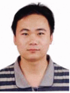 Liang Chen (陈亮)合作论文数31
 Yanxiao Zhao (赵彦晓)合作论文数Department of Electrical and Computer Engineering, College of Engineering, Virginia Commonwealth University24
 Fu Qiang合作论文数20Yaohai Cheng合作论文数18Jun-Ning Gan合作论文数18li zhiguo合作论文数17Lijian He合作论文数16huo wenjuan (霍文娟)合作论文数15
 Huang Lu合作论文数15Ying Xiao (肖盈)合作论文数15Zhiyi Lu合作论文数15Yujie Zhang (张瑜洁)合作论文数15
 Yi-Wen Huang合作论文数Iowa15LiangHao Zhang (张良浩)合作论文数14Yinghua Sun (孙英华)合作论文数Beijing University of Technology14Zhiyun Jiang (江之韵)合作论文数13Li Jia合作论文数13RenQing Wang (王任卿)合作论文数13
 Ke Liu (刘克)合作论文数The Key Laboratory of Optoelectronics Technology, Beijing University of Technology13
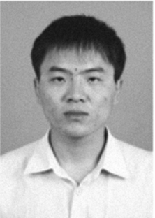 Ning Hu合作论文数13Dong Lu (鲁东)合作论文数12Dong Gao (高栋)合作论文数12Zhang Wei (张蔚)合作论文数12YongPing Sha合作论文数11JianJun Qiu合作论文数11Shuo Liu (刘硕)合作论文数11Xinyi Zhao合作论文数11
 Guangdi Shen (沈光地)合作论文数Optoelectronics Technology Laboratory, Beijing University of Technology11Yanling GUO (郭燕玲)合作论文数10GuangHui Xing (邢光辉)合作论文数10QingYuan Zhang (张卿远)合作论文数10RuiXin Hu (胡瑞心)合作论文数10Xin Huang (黄鑫)合作论文数10Zhenjie Guo (郭振杰)合作论文数10
 Qiang Fu (付强)合作论文数Department of Atmospheric Sciences, College of the Environment, University of Washington10Menglong Zhou合作论文数9Xiaoting Shen合作论文数9Wang Yang合作论文数9Xin ZHAO (赵昕)合作论文数9Yang Xiang (向洋)合作论文数8Yang Jing-wei合作论文数8Yin Sha合作论文数8Pan Gao合作论文数8Xiao Wang合作论文数8




