An optical feedback cavity ring down (OF-CRD) technique for simultaneously measuring the S-(perpendicular to the plane of incidence) and P-(in the plane of incidence) polarization reflectivity of highly reflective coatings is developed. Polarized light with a certain ratio of S- and P-polarization power and with square-wave modulated intensity is coupled into a ring-down cavity. The ring-down signal that leaks out from a cavity mirror is recorded at the negative edge of the modulation and fitted to a bi-exponential function to determine simultaneously the ring-down time for S and P polarizations. The reflection coefficients of highly reflective coatings for the S and P polarizations are therefore calculated from the determined ring-down time. Compared to the results obtained with purely S or P polarization, the differences for both S and P polarizations are respectively 1 ppm and 15 ppm, indicating the correctness of the simultaneous measurements. Compared to the conventional CRD approach, this simultaneous measurement method has the advantages of simpler configuration, easier operation, and higher speed.
As an increasing amount of functionality is crammed into today's mobile phones, designers must find ways to save board area. Two common solutions are the use of embedded passives and the use of smaller (0201) discretes. In this paper, we examine the cost and area tradeoffs between small discretes and embedded polymer thick resistors. Three typical mobile phone designs are analyzed using high volume assembly and state of the art board fabrication techniques for scenarios with either small discretes or polymer thick film (PTF) resistors. The size and cost impacts of each option are presented.
In recent years,following the driver IC’s I/O numbers are becoming higher, the density of IC’s bμmps is becoming greater. For suiting these fine pitch bumps, the width/space of COF substrate is smaller than 50μm commonly and especially some width/space of ILB(Inner Line Bonding) has decreased to 15μm. Because of the unavoidable side etching, it is difficult to produce these fine lines by conventional subtractive process. The semi- additive process is more suitable for forming finer pattern because it is able to inhibit side etching greatly. In this paper, we have used sputtered FCCL with 2μm copper layer to produce two kinds of fine line substrates which are 50μm/50μm and 30μm/30μm by semi-additive process. In flash etching of the semi-additive process, we made use of not HCl/CuCl2 etchant but H2SO4/H2O2 etchant to etch the base copper. The semi-additive process has a good etching performance and the section of lines formed by it closely resemble rectangles. Even the width/space decreased from 50μm/50μm to 30μm/30μm, the section of pattern formed by semi-additive process is also ideal. and doesn’t become trapeziform.At the same time, because the etching time in semi-additive process is very short, it leads to a better conductor width retention. So the width/space is closed to the design size.
The paper introduces the way of embedding of passive and active components into FPC. Thin filmresistors can be embedded by electroless deposited Ni(P) resistors and the thin film resistors have considerableflexibility. The embedded active chip also can be realized by backside thinning and flip chip bonding. Then, thereliability of the components have been tested.
This paper describes the research that has lead to a software tool that predicts the thermal behaviour of embedded passive components in multilayer PCBs. Internal component models are generated using the Transmis- sion Line Matrix (TLM) diffusion method. Individual components can contain hundreds of temperature calculation points and are modelled in 3-Dimensions. High resolution board detail is also achieved, with a board typically contain- ing over 100,000 temperature calculation nodes. The software then uses the results from this 3-D data to build up detailed component and board level thermal design rules. The paper also touches on how the software takes into account additional thermal aspects such as board structure, including thickness and position of copper planes and the other aspects of surface mounted components.
Optomec is developing a new printing method, known as M3DTM, for depositing high precision PTF resistors. This new approach produces resistors with a variability of better than 10% in the range of 100?-10k? and at a footprint below 0.05mm2. M3DTM allows the locations and resistance values to be determined from the CAD file, which eliminates the need for creating screens or stencils and eliminates trimming requirements. It is a cost-effective solution for printing embedded resistors.
Technology development for embedding of passive components has been the subject of significant focus for OEMs, board fabs and material suppliers for the past few years. This has been driven primarily by the need to miniaturize portable devices like mobile phones though performance advantages accruing from embedding passives is also becoming increasingly significant. DuPont's focus in the area of Embedded Passives has been on the development of resistive and capacitive materials for applications in organic substrates. The product family includes a wide range of materials viz. ceramic and polymer thick-film capacitor and resistor pastes for discrete embedded devices and filled and unfilled organic laminates for applications requiring planar capacitance. Previous publications have described the technology development involving standard thick-film and printed wiring boards (PWB) processes to embed thick-film ceramic passives in PWBs. This paper focuses on reliability of embedded thick film ceramic capacitors.
The paper introduces the 3MTM Embedded Capacitor Material’s advantages when the material is utilized in embedded passives. 3MTM Embedded Capacitor Material has excellent electrical performance, and has been success- fully implemented on OEM designs to replace large quantities of discrete decoupling capacitors from the board surface and obviously reduce board size. It has the visible impact on system cost. And the material is compatible with standard flex and rigid PCB materials and processing, passing all the industry reliability tests.
Many articles have been published on the benefit of thin substrates for use as embedded capacitor layers as well as thin film resistive material for embedded resistors.Until now the utilization of both technologies within a printed circuit design required the use of separate cores within the PCB.This adds additional thickness to the PCB as well as cost.A new substrate has been developed to address these issues.Embedded technologies improve the electri-cal performance of high speed digital circuits as well as enabling the removal of SMT discrete components.By combin-ing capacitance and resistance on the same core,with the resistor foil being supplied on one or bothsides of the capacitor dielectric,these benefits can be realized without increasing the overall number of layers or the substrate thickness.Also,some unique R-C circuit designs can be formed by utilizing this substrate.We will discuss the process and design guidelines for using this substrate as well as some possible applications.Also,results from high frequency testing of PCB test vehicles will be discussed.Future product developments will also be shared.It will be demonstrated that this new substrate has excellent electrical properties while being able to be readily manufactured using typical inner-layer processing.
The trend that electronic products become more diminutive and more lightsized continues.So,various flat panel display are applied widely,the LCD panel is a prominent type.the COF technology has become the primary packaging technique for driver IC of LCD by many advantages owned by it.In this paper,the structure,features,key process,applications and developing direction of COF are summarized.
 JingHao Xu (徐景浩)合作论文数10XuanDong Zhang (张宣东)合作论文数10
 Bo He (何波)合作论文数School of Economics and Business Administration, Chongqing University9
 Wei He (何为)合作论文数University of Electronic Science and Technology of China8Jian Guan (关健)合作论文数6YunQi Mo (莫芸绮)合作论文数3Shilei Xiao合作论文数1ZHAO Li (赵丽)合作论文数1
 Guoyun Zhou (周国云)合作论文数School of Materials and Energy, University of Electronic Science and Technology of China1
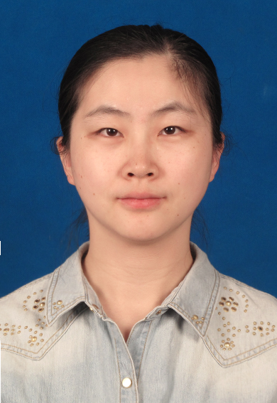 Jing Wang (王静)合作论文数School of Optoelectronic Science and Engineering, University of Electronic Science and Technology of China1
 Chunming Gao (高椿明)合作论文数School of Optoelectronic Science and Engineering, University of Electronic Science and Technology of China1
 Yafei Wang (王亚非)合作论文数School of Optoelectronic Science and Engineering, University of Electronic Science and Technology of China1
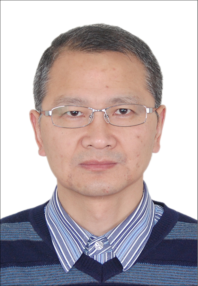 Bincheng Li (李斌成)合作论文数School of Optoelectronic Science and Engineering, University of Electronic Science and Technology of China1Songlun Liu (刘松伦)合作论文数1




