We present and discuss the performance characteristics of InP-based p-i-n photodiodes (PDs) with InGaAs/GaAsSb type-II multiple quantum wells absorption regions designed to absorb light at mid-infrared wavelengths. Top-illuminated and waveguide-integrated PDs are fabricated with dark currents as low as 100 nA at -2 V, an external responsivity as high as 0.27 A/Wat 2 mu m and 0.3 A/Wat 1.55 mu m, and a 3-dB bandwidth of 3.5 GHz at 2 mu m.
We present a high-speed integrated waveguide photodetector exhibiting a dark current of 2 nA at −2 V with an internal responsivity of 0.25 A/W and a 3-dB bandwidth above 8 GHz at 2 μm wavelength.
Waveguide-integrated photodiodes with InGaAs/GaAsSb type-II quantum well absorption regions designed to absorb light at 2 mu m are presented. A novel dual-integrated waveguide-depletion layer was used to maximize quantum efficiency in photodiodes designed with thin absorbers for high-speed optical response. Low dark currents (1 nA at -1 V) and an internal responsivity of 0.84 A/W along with a bandwidth above 10 GHz and an open eye diagram at 10 Gb/s have been demonstrated at 2 mu m. The high-speed carrier dynamics within InGaAs/GaAsSb type-II quantum wells are explored for the first time and suggest that the transit time of the photodiode is limited by light hole escape times in the quantum wells.
We present a high-speed InP-based photodiode with multiple InGaAs/GaAsSb type-II quantum wells for 2 μm detection. The fabricated photodiode exhibits dark current as low as 100nA at -2V, with an external responsivity of 0.27 A/W, and 3 dB bandwidth of 3.5 GHz at 2 μm.
We present an InP-based p-i-n photodiode with multiple InGaAs/GaAsSb type-II quantum wells for 2 μm detection. The fabricated photodiode shows a responsivity of 0.24 A/W at 2 μm, with dark current as low as 1 μA at -2 V, and 3 dB-bandwidth of 2 GHz under 1.55 μm optical illumination.
InP-based strained-well InGaAs/GaAsSb quantum well photodiodes with non-zero net strain can be used to extend detection wavelengths well into the mid-infrared region. However, excess dark current due to defects in the structure can be a performance limiting factor in photodiodes of this type. In this reported work, both low-frequency noise spectroscopy and deep level transient spectroscopy were used to investigate traps in prototypical strained-well photodiode heterostructures. Two distinct traps were identified and their electrical and physical properties and distributions have been evaluated.
Interactive Panel on Perspectives and Practical Skills for Men as Advocates for Gender EquityMany factors – systemic and non-systemic, conscious and unconscious, policy and climate – cannegatively impact the participation of minority group members in an organization. Particularlywhen a majority group is highly dominant, these barriers pervade recruitment, retention,advancement, and overall climate; diversity suffers, and the overall effectiveness and health ofthe organization is diminished. Academia has a long history of dominance by men. This hasbeen and remains particularly true in engineering.There is a growing body of evidence that men and majority individuals can serve crucial roles tosupport the advancement of women within organizations. To be effective, however, requiresbroad commitment and intentional and informed advocacy. Unfortunately, there are many forcesthat undermine men’s participation as advocates, including apathy, lack of knowledge, and fear.Men, especially those with a record of effective advocacy, can help promote men’s engagementas advocates.This panel will bring together a group of men with diverse backgrounds and experiences todiscuss their perspectives and offer practical skills for men to effectively serve as advocates forgender equity. Panelist discussion will focus on 1) awareness of issues, including unconscious bias, male privilege, and unearned advantage 2) individual-level advocacy: barriers and opportunities 3) institution-level advocacy: barriers and opportunities 4) advocacy best practices, including a focus on male advocates working with other men 5) examples of effective advocacy in actionA paper will be compiled that captures the background of utilizing men as advocates for genderequity; describes the panelist’s perspectives, experiences, and recommendations for effectiveadvocacy; and concludes by identifying common themes, advocacy best-practices, and how totake the first steps to get involved.Panel attendees, particularly men and administrators, will benefit by understanding barriers toadvocacy, learning best-practices of effective advocacy, and hearing first-hand experiences ofsuccessful advocacy.
In foundational knowledge engineering courses, students engage in problem solving in order to learn important course concepts. To help in this process, students receive feedback on their performance from the instructor. This paper explores an alternative to instructor-provided feedback: a semi-structured assignment in which students reworked problems they failed to solve correctly on a midterm exam for credit. The assignment required students to provide a correct solution to the problem and identify both mathematical and conceptual errors made in the initial solution. The initial results show that students who completed this assignment were able to apply course concepts in analysis and reasoning questions more accurately than students who received exam feedback from the instructor. In addition, these students showed a marked improvement in their ability to solve problems common in a Circuit Analysis course. These results show that such semi-structured assignments can replace instructor-provided feedback in large-enrollment classes and lead to improved problem solving.
This paper discusses the effects of using frequent online quizzes as a replacement for homework in an Electric Circuits Course. The results of two experiments show that performance on these quizzes is correlated with performance on course exams, conceptual understanding of the material, and problem solving ability. These results do not appear to be correlated with prior knowledge, grit, or self-efficacy.
A novel InP-based multispectral photodetector chip, using multiple Fabry-Perot resonant cavities integrated with photodectors, was designed, fabricated, and characterized. The integrated devices are capable of simultaneous wavelength detection at four wavelengths in the near infrared/short-wave infrared regime such as 1.32, 1.41, 1.49, and 1.66 μm. Experimental results show highly distinguishable detection peaks from 22.8% to 37.4%. A little change in dark current density has been observed after filter integration (~2χ10-2 A/cm2 at -10 V). The experimental full-width half-maximum values are 2.18-2.9 times of the design's, indicating light scattering caused by cavity etch and cavity thickness nonuniformities. The discrepancy between design and experimental results are analyzed for a better understanding of the filter properties and experimental variables.
As engineering disciplines evolve, universities are challenged to continually incorporate new material into the undergraduate curriculum. Traditionally, the two primary methods of incorporating new material are to either change the curriculum of a specific class or hire a new instructor to teach a new class. In our paper, we introduce a new model for introducing skills and tools necessary for undergraduates to succeed in industry/academia via the Student Taught Classes program (STC). Overall, the STC program has been widely successful and far reaching. The popularity of the program can be attributed to the rigorous application process, flexible class structure, and broad impact that each of the seven classes taught have had over the past three semesters. When instituted in the right way, Student Taught Classes have the ability to add a new dimension to any undergraduate engineering curriculum.
We report on InP-based p-type/intrinsic/n-type (PIN) photodiodes with a novel strain-compensated type-II InGaAs/GaAsSb quantum well active region. The device has optical response out to 3.0 μm, specific detectivity (D*) of 7.73×10(9) cm Hz(0.5)/W at 290 K for 2.7 μm. These preliminary results show that this novel strain-compensated approach leads to similar performance when compared to a conventional strain-compensated approach.
This paper reports the dark current characteristics of SWIR and MWIR p–i–n photodiodes with type-II InGaAs/GaAsSb multiple quantum wells as the absorption region. A bulk based model with the effective band gap of the type-II quantum well structure has been used. We investigated the dark current contributing mechanisms that are limiting the electrical performance of these photodiodes. The quantitative simulation of the I–V characteristics shows that the performance of InGaAs/GaAsSb photodiodes is dominated by generation-recombination component at the temperature between 200 and 290 K for reverse biases below 5 V. Trap-assisted tunneling current and direct tunneling current begin to dominate when the reverse bias is higher than 10 V.
Optical gain performance of InP based “W” structure with InGaAs(N)/GaAsSb type-II quantum wells are investigated theoretically. The band structure was calculated by using k.p model, taking into account the conduction band mixing with N resonant band, valence band mixing, as well as strain effect. Our studies show that these type-II quantum wells are suitable for mid-infrared (2–4 μm) operation at room temperature.
In this paper, a new method of studying the carrier transport is proposed and demonstrated. We designed two structures to study the carrier transport mechanism in InP-based photodiodes with InGaAs/GaAsSb type-II quantum well absorption regions. Based on the comparison of the responsivity of the two different device structures, we concluded that thermionic emission is the dominant carrier transport mechanism for these quantum well structures.
Multiple quantum well (MQW) photodiodes based on the InGaAs/GaAsSb material system are emerging as viable candidates for mid infrared detection. A critical issue for these devices is dark current caused by defects within the material. In this work, low frequency noise spectroscopy and random telegraph signal characterization were used to characterize defect levels in MQW photodiodes. Three traps, located at 0.14 eV (E-a), 0.34 eV (E-b), and 0.43 eV (E-c), were identified from the measured noise. E-a is associated with bulk InGaAs, E-b may be associated with bulk GaAsSb, and E-c is localized at the InGaAs/GaAsSb heterointerface. (C) 2012 American Institute of Physics. [http://dx.doi.org/10.1063/1.4740275]
Monte Carlo simulation is performed on a low-noise, three-stage tandem avalanche photodiode with InAlAs/InAlGaAs impact-ionization-engineered multiplication region. The simulated excess noise factor agrees well with experimental measurements. A modified structure to further reduce the excess noise is proposed.
Different type-II InGaAs/GaAsSb quantum well design structures on InP substrate for mid-infrared emission has been modeled by six band k•p method. The dispersion relations, optical matrix element, optical gain and spontaneous emission rate are calculated. The effects of the parameters of quantum wells (thickness, composition) and properties of cladding layers were investigated. For injected carrier concentration of 5×1012 cm-2, peak gain values around 2.6-2.7 μm wavelengths of the order of 1000 cm-1 can be achieved, which shows that type-II InGaAs/GaAsSb quantum wells are suitable for infrared laser operation beyond 2μm at room temperature.
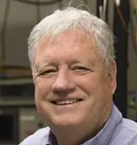 Joe Charles Campbell合作论文数School of Engineering and Applied Science, University of Virginia58
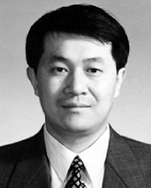 Xiaoguang Zheng合作论文数Electrical and Computer Engineering Department, University of Virginia26
 Rubin Sidhu合作论文数24
 Michael M. Oye合作论文数Microelectronics Research Center and Texas Materials Institute, The University of Texas at Austin22
 Steven P. Denbaars合作论文数Solid State Lighting & Energy Electronics Center, University of California, Santa Barbara22
 Baile Chen (陈佰乐)合作论文数School of Information Science and Technology, ShanghaiTech University19
 Geoffrey S. Kinsey合作论文数Spectrolab , Inc18Ben G. Streetman合作论文数15
 Russell Dean Dupuis合作论文数School of Electrical and Computer Engineering, College of Engineering, Georgia Institute of Technology15
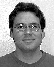 Jeffrey B. Hurst合作论文数14Jason M. Reifsnider合作论文数14
 Jinrong Yuan合作论文数13
 John Bowers合作论文数Department of Electrical and Computer Engineering, College of Engineering, University of California, Santa Barbara12
 Larry A. Coldren合作论文数Optoelectronics Technology Center, Department of Electrical & Computer Engineering, College of Engineering, University of California, Santa Barbara12Baklenov, O.合作论文数11
 Feng Ma合作论文数11
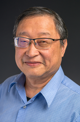 Chih-Kang Shih合作论文数Department of Physics, College of Natural Sciences, University of Texas at Austin10Govindaraju Santhosh合作论文数Central College Campus, Bangalore University10Terry J. Mattord合作论文数10
 Xiaoli Sun合作论文数Goddard Space Flight Center, National Aeronautics and Space Administration9
 Shuling Wang合作论文数Microelectronics Research Center;Department of Electrical and Computer Engineering;University of Texas at Austin;Microelectronics Research Center, University of Texas at Austin9Gauri Karve合作论文数9
 Evelyn Hu (胡玲)合作论文数John A. Paulson School of Engineering and Applied Sciences, Harvard University;Hong Kong Institute for Advanced Study, City University of Hong Kong9m e heimbuch合作论文数8
 Xiaoguang Sun (孙晓光)合作论文数8Islam, M.R.合作论文数8
 Andrew S. Huntington合作论文数8D. Gotthold合作论文数Emcore Corporation8
 S. Wang合作论文数7Xw Li合作论文数7
 Casper M. Reaves合作论文数7
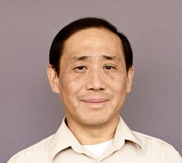 Han Htoon合作论文数Center for Integrated Nanotechnologies, Los Alamos National Laboratory7H. Nie合作论文数6Ning Duan合作论文数6Peng Xi Yuan合作论文数6
 Xiaoping Yang (杨小平)合作论文数College of Chemistry & Materials Engineering, Wenzhou University6
 Ning Li (李宁)合作论文数6
 Richard A Jones合作论文数Center for Electrochemistry, Department of Chemistry, College of Natural Sciences, The University of Texas at Austin6F. J. Ciuba合作论文数6Sridhar Govindaraju合作论文数Texas Materials Institute and Microelectronics Research Center, The University of Texas at Austin6C Hansing合作论文数6K. G. Fertitta合作论文数6W. Y. Jiang合作论文数5d g yu合作论文数5dmitrii a kulik合作论文数5
 Bassem Tossoun合作论文数Hewlett Packard Enterprise, Hewlett Packard Labs5
 Sadhvikas Addamane合作论文数Sandia Natl Labs, Ctr Integrated Nanotechnol, Albuquerque, NM 87185 USA5
 Ganesh Balakrishnan合作论文数Ctr High Technol Mat, Univ New Mexico5William P. Risk合作论文数5




