Native mass spectrometry (MS) has become widely accepted in structural biology, providing information on stoichiometry, interactions, homogeneity, and shape of protein complexes. Yet, the fundamental assumption that proteins inside the mass spectrometer retain a structure faithful to native proteins in solution remains a matter of intense debate. Here, we reveal the gas-phase structure of β-galactosidase using single-particle cryo–electron microscopy (cryo-EM) down to 2.6-Å resolution, enabled by soft landing of mass-selected protein complexes onto cold transmission electron microscopy (TEM) grids followed by in situ ice coating. We find that large parts of the secondary and tertiary structure are retained from the solution. Dehydration-driven subunit reorientation leads to consistent compaction in the gas phase. By providing a direct link between high-resolution imaging and the capability to handle and select protein complexes that behave problematically in conventional sample preparation, the approach has the potential to expand the scope of both native mass spectrometry and cryo-EM.
Native mass spectrometry (native MS) is a powerful technique that provides information on stoichiometry, interactions, homogeneity and shape of protein complexes. However, the extent of deviation between protein structures in the mass spectrometer and in solution remains a matter of debate. Here, we uncover the gas-phase structure of β-galactosidase using single particle electron cryomicroscopy (cryo-EM) down to 2.6 Å resolution, enabled by soft-landing of mass-selected protein complexes onto cold TEM grids and in-situ ice coating. We find that large parts of the secondary and tertiary structure are retained from solution, with dehydration-driven subunit reorientation leading to consistent compaction in the gas phase. Our work enables visualizing the structure of gas-phase protein com-plexes from numerous experimental scenarios at side-chain resolution and demonstrates the possibility of more controlled cryo-EM sample preparation. One Sentence Summary Electrospray ion-beam deposition on cold grids and in-vacuum ice growth enable cryo-EM of mass-selected proteins at 2.6 Å.
Journal Article Merging Machine Learning and TriBeam Tomography for 3D Defect Detection in an AM CoNi-Based Superalloy Get access James Lamb, James Lamb University of California Santa Barbara, Materials Department, Santa Barbara, CA, United States Corresponding author: jlamb@ucsb.edu Search for other works by this author on: Oxford Academic Google Scholar McLean Echlin, McLean Echlin University of California Santa Barbara, Materials Department, Santa Barbara, CA, United States Search for other works by this author on: Oxford Academic Google Scholar Andrew Polonsky, Andrew Polonsky Sandia National Laboratories, Materials Mechanics & Tribology, Albuquerque, NM, United States Search for other works by this author on: Oxford Academic Google Scholar Remco Geurts, Remco Geurts Thermo Fisher Scientific, Eindhoven, Netherlands Search for other works by this author on: Oxford Academic Google Scholar Kira Pusch, Kira Pusch University of California Santa Barbara, Materials Department, Santa Barbara, CA, United States Search for other works by this author on: Oxford Academic Google Scholar Evan Raeker, Evan Raeker University of California Santa Barbara, Materials Department, Santa Barbara, CA, United States Search for other works by this author on: Oxford Academic Google Scholar Aurelien Botman, Aurelien Botman Thermo Fisher Scientific, Hillsboro, OR, United States Search for other works by this author on: Oxford Academic Google Scholar Chris Torbet, Chris Torbet University of California Santa Barbara, Materials Department, Santa Barbara, CA, United States Search for other works by this author on: Oxford Academic Google Scholar Tresa Pollock Tresa Pollock University of California Santa Barbara, Materials Department, Santa Barbara, CA, United States Search for other works by this author on: Oxford Academic Google Scholar Microscopy and Microanalysis, Volume 28, Issue S1, 1 August 2022, Pages 862–863, https://doi.org/10.1017/S1431927622003828 Published: 01 August 2022
Journal Article Observations of Damage, Defects, and Structuring in Femtosecond Laser Ablated Surfaces Get access McLean P Echlin, McLean P Echlin University California Santa Barbara, Materials Department, Santa Barbara, California, USA Corresponding author: mechlin@ucsb.edu Search for other works by this author on: Oxford Academic Google Scholar Andrew T Polonsky, Andrew T Polonsky Sandia National Laboratories, Materials Mechanics & Tribology, Albuquerque, New Mexico, USA Search for other works by this author on: Oxford Academic Google Scholar Will C Lenthe, Will C Lenthe EDAX / Ametek, Mahwah, New Jersey, USA Search for other works by this author on: Oxford Academic Google Scholar Mike S Titus, Mike S Titus Purdue University, Lafayette, Indiana, USA Search for other works by this author on: Oxford Academic Google Scholar Remco Geurts, Remco Geurts Thermo Fisher Scientific, Eindhoven, Netherlands Search for other works by this author on: Oxford Academic Google Scholar Aurélien Botman, Aurélien Botman Thermo Fisher Scientific, Hillsboro, Oregon, United States Search for other works by this author on: Oxford Academic Google Scholar Marcus Straw, Marcus Straw Applied Physics Technologies, McMinnville, Oregon, United States Search for other works by this author on: Oxford Academic Google Scholar Peter Gumbsch, Peter Gumbsch Karlsruhe Institute of Technology, Karlsruhe, GermanyFraunhofer-Institut für Werkstoffmechanik IWM, Freiburg, Germany Search for other works by this author on: Oxford Academic Google Scholar Tresa M Pollock Tresa M Pollock University California Santa Barbara, Materials Department, Santa Barbara, California, USA Search for other works by this author on: Oxford Academic Google Scholar Microscopy and Microanalysis, Volume 28, Issue S1, 1 August 2022, Pages 872–873, https://doi.org/10.1017/S1431927622003865 Published: 01 August 2022
Streams of multimodal three-dimensional (3D) and four-dimensional (4D) data are revolutionizing our ability to design and predict the behavior of a broad array of advanced materials systems. Over the last 10 years, a new 3D imaging platform consisting of a femtosecond (fs) pulsed laser coupled with a focused ion beam scanning electron microscope (FIB SEM) has been developed by UC Santa Barbara in collaboration with Thermo Fisher Scientific (formerly FEI). The femtosecond-laser-enabled FIB SEM, called the TriBeam, has become one of the only 3D serial sectioning methods available that can gather millimeter-scaled multimodal datasets at sub- $$\mu $$ m voxel resolutions; these length scales are critical for many materials problems. Multimodal chemical, crystallographic, and morphological information can be gathered rapidly on a layer-by-layer basis and reconstructed in 3D. Large (gigabyte to terabyte scale) 3D datasets have been generated for a broad array of materials systems, including metallic alloys, ceramics, biomaterials, polymer- and ceramic-matrix composites, and semiconductors. The research tasks performed have resulted in a completely new design, operating with a dual-wavelength femtosecond-pulsed laser on a plasma focused ion beam (PFIB) platform.
Correlative light and electron microscopy (CLEM) is a powerful tool for defining the ultrastructural context of molecularly-labeled biological specimens, particularly when superresolution fluorescence microscopy (SRM) is used for CLEM. Current CLEM, however, is limited by the stark differences in sample preparation requirements between the two modalities. For CLEM using SRM, the small region of interest (ROI) of either or both modalities also leads to low success rate and imaging throughput. To overcome these limitations, here we present a CLEM workflow based on a novel focused ion beam/scanning electron microscope (FIB/SEM) compatible with common SRM for imaging biological specimen with ultrahigh 3D resolution and improved imaging throughput. By using a reactive oxygen source in a plasma FIB (PFIB) and a rotating sample stage, the novel FIB/SEM was able to achieve several hundreds of micrometer large area 3D analysis of resin embedded cells through a process named oxygen serial spin mill (OSSM). Compared with current FIB mechanisms, OSSM offers gentle erosion, highly consistent slice thickness, reduced charging during SEM imaging, and improved SEM contrast without increasing the dose of post-staining and fixation. These characteristics of OSSM-SEM allowed us to pair it with interferometric photoactivated localization microscopy (iPALM), a recent SRM technique that affords 10–20 nm isotropic spatial resolution on hydrated samples, for 3D CLEM imaging. We demonstrate a CLEM workflow generalizable to using other SRM strategies using mitochondria in human osteosarcoma (U2OS) cells as a model system, where immunostained TOM20, a marker for the mitochondrial outer membrane, was used for iPALM. Owing to the large scan area of OSSM-SEM, it is now possible to select as many FOVs as needed for iPALM and conveniently re-locate them in EM, this improving the imaging throughput. The significantly reduced dose of post-fixation also helped to better preserve the sample ultrastructures as evidenced by the excellent 3D registration between OSSM-SEM and iPALM images and by the accurate localization of TOM20 (by iPALM) to the peripheries of mitochondria (by OSSM-SEM). These advantages make OSSM-SEM an ideal modality for CLEM applications. As OSSM-SEM is still in development, we also discuss some of the remaining issues and the implications to biological imaging with SEM alone or with CLEM.
Nickel nanostructures have found widespread application as both functional components, e.g. in magnetic systems, and as part of the lithographic pattern transfer process as etch masks, EUV mask absorbers, and imprint templates. Electron-beam induced etching of nickel is highly desirable for the repair and editing of masks and templates with high resolution and without substrate damage. However, there are no known gas-phase reactants that produce volatile nickel products under e-beam irradiation. Here we report the successful local etching of nickel by a focused electron beam in an environmental scanning electron microscope using aliquidreactant, aqueous sulfuric acid. Sulfuric acid did not spontaneously etch nickel under ESEM conditions, but nickel was etched in areas exposed to the electron beam. Etching parameters such as dose, refresh time, and addition of a surfactant were investigated. The extent of the etch increases with dose before terminating at sub-micron feature sizes. The etch resolution improves with the addition of surfactant. This approach enables local nickel patterning with complete film removal but without damaging underlying layers. With further refinement, the process may enable nickel absorber repair and editing and remove a significant obstacle to the use of nickel in EUV lithography.
Journal Article TriBeam Tomography for 3D Data Acquisition Get access McLean Echlin, McLean Echlin University California-Santa Barbara, San Francisco, California, United States Search for other works by this author on: Oxford Academic Google Scholar Andrew Polonsky, Andrew Polonsky University California-Santa Barbara, San Francisco, California, United States Search for other works by this author on: Oxford Academic Google Scholar Toby Francis, Toby Francis University California-Santa Barbara, San Francisco, California, United States Search for other works by this author on: Oxford Academic Google Scholar Will Lenthe, Will Lenthe Carnegie Mellon University, Pittsburgh, Pennsylvania, United States Search for other works by this author on: Oxford Academic Google Scholar Mike Titus, Mike Titus Purdue University, West Lafayette, Indiana, United States Search for other works by this author on: Oxford Academic Google Scholar Alessandro Mottura, Alessandro Mottura Birmingham University, Birmingham, England, United Kingdom Search for other works by this author on: Oxford Academic Google Scholar Chris Torbet, Chris Torbet University California-Santa Barbara, San Francisco, California, United States Search for other works by this author on: Oxford Academic Google Scholar Steven Randolph, Steven Randolph Thermo Fisher Scientific, Hillsboro, Oregon, United States Search for other works by this author on: Oxford Academic Google Scholar Aurelien Botman, Aurelien Botman Thermo Fisher Scientific, Hillsboro, Oregon, United States Search for other works by this author on: Oxford Academic Google Scholar Jorge Filevich, Jorge Filevich Thermo Fisher Scientific, Hillsboro, Oregon, United States Search for other works by this author on: Oxford Academic Google Scholar ... Show more Remco Geurts, Remco Geurts Thermo Fisher Scientific, Eindhoven, Noord-Brabant, Netherlands Search for other works by this author on: Oxford Academic Google Scholar Marcus Straw, Marcus Straw Applied Physics Technology, McMinnville, Oregon, United States Search for other works by this author on: Oxford Academic Google Scholar Tresa Pollock Tresa Pollock University California-Santa Barbara, San Francisco, California, United States Search for other works by this author on: Oxford Academic Google Scholar Microscopy and Microanalysis, Volume 26, Issue S2, 1 August 2020, Pages 2624–2625, https://doi.org/10.1017/S1431927620022229 Published: 01 August 2020
Journal Article 3D Characterization of a Novel CoNi-superalloy for Additive Manufacturing Get access Andrew Polonsky, Andrew Polonsky University of California-Santa Barbara, Santa Barbara, California, United States Search for other works by this author on: Oxford Academic Google Scholar Toby Francis, Toby Francis University of California-Santa Barbara, Santa Barbara, California, United States Search for other works by this author on: Oxford Academic Google Scholar Kira Pusch, Kira Pusch University of California-Santa Barbara, Santa Barbara, California, United States Search for other works by this author on: Oxford Academic Google Scholar McLean Echlin, McLean Echlin University of California-Santa Barbara, Santa Barbara, California, United States Search for other works by this author on: Oxford Academic Google Scholar Aurelien Botman, Aurelien Botman Thermo Fisher Scientific, Hillsboro, Oregon, United States Search for other works by this author on: Oxford Academic Google Scholar Steven Randolph, Steven Randolph Thermo Fisher Scientific, Hillsboro, Oregon, United States Search for other works by this author on: Oxford Academic Google Scholar Remco Geurts, Remco Geurts Thermo Fisher Scientific, Eindhoven, Noord-Brabant, Netherlands Search for other works by this author on: Oxford Academic Google Scholar Jorge Filevich, Jorge Filevich Thermo Fisher Scientific, Hillsboro, Oregon, United States Search for other works by this author on: Oxford Academic Google Scholar Tresa Pollock Tresa Pollock University of California-Santa Barbara, Santa Barbara, California, United States Search for other works by this author on: Oxford Academic Google Scholar Microscopy and Microanalysis, Volume 26, Issue S2, 1 August 2020, Pages 1688–1690, https://doi.org/10.1017/S1431927620018978 Published: 01 August 2020
The authors have developed a system combining a 220 fs pulse focused laser beam operating at 1030 or 515 nm, a Xe+ plasma source focused ion beam, and a Schottky source focused electron beam, all coincident at the sample. They present on results and applications for in situ micro device characterization and large volume 3D analysis.
Ultra-nanocrystalline diamond (UNCD) is increasingly being used in the fabrication of devices and coatings due to its excellent tribological properties, corrosion resistance, and biocompatibility. Here, we study its response to irradiation with kiloelectronvolt electrons as a controlled model for extreme ionizing environments. Real time Raman spectroscopy reveals that the radiation-damage mechanism entails dehydrogenation of UNCD grain boundaries, and we show that the damage can be recovered by annealing at 883 K. Our results have significant practical implications for the implementation of UNCD in extreme environment applications, and indicate that the films can be used as radiation sensors.
Recent advances in focused ion beam technology have enabled high-resolution, direct-write nanofabrication using light ions. Studies with light ions to date have, however, focused on milling of materials where sub-surface ion beam damage does not inhibit device performance. Here we report on direct-write milling of single crystal diamond using a focused beam of oxygen ions. Material quality is assessed by Raman and luminescence analysis, and reveals that the damage layer generated by oxygen ions can be removed by nonintrusive post-processing methods such as localised electron beam induced chemical etching.
We show here that copper can be locally etched by an electron-beam induced reaction in a liquid. Aqueous sulfuric acid (H2SO4) is utilized as the etchant and all experiments are conducted in an environmental scanning electron microscope. The extent of etch increases with liquid thickness and dose, and etch resolution improves with H2SO4 concentration. This approach shows the feasibility of liquid phase etching for material selectivity and has the potential for circuit editing.
AbstractThe introduction of gases, such as water vapor, into an environmental scanning electron microscope is common practice to assist in the imaging of insulating or biological materials. However, this capability may also be exploited to introduce, or form, liquid phase precursors for electron-beam-induced deposition. In this work, the authors report the deposition of silver (Ag) and copper (Cu) structures using two different cell-less in situ deposition methods—the first involving the in situ hydration of solid precursors and the second involving the insertion of liquid droplets using a capillary style liquid injection system. Critically, the inclusion of surfactants is shown to drastically improve pattern replication without diminishing the purity of the metal deposits. Surfactants are estimated to reduce the droplet contact angle to below ~10°.
 Steven Randolph合作论文数10Straw Marcus合作论文数9
 Milos Toth合作论文数School of Mathematical and Physical Sciences, University of Technology Sydney9J. J. L. Mulders合作论文数8Remco Geurts合作论文数5
 McLean Echlin合作论文数Materials Department, College of Engineering, University of California, Santa Barbara5Jorge Filevich合作论文数Departamento de Física;Facultad de Ciencias Exactas;Universidad de Buenos Aires;Facultad de Ciencias Exactas, Naturales Universidad de Buenos Aires5Steven J. Randolph合作论文数4
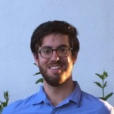 Andrew T. Polonsky合作论文数Materials Department,University of California Santa Barbara,Santa Barbara,USA4
 Tresa M. Pollock合作论文数University of California, Santa Barbara4
 Kees Hagen合作论文数Department of Imaging Physics, Faculty of Applied Sciences, Delft University of Technology3
 J. T. Hastings合作论文数NanoStructures Laboratory, Massachusetts Institute of Technology3M Hesselberth合作论文数2Chris J. Torbet合作论文数2James Lamb合作论文数2
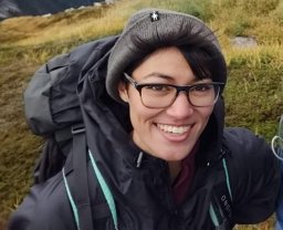 Kira Pusch合作论文数Mat Dept, Univ Calif Santa Barbara2
 Toby Francis合作论文数Univ Calif Santa Barbara2Márkó Grabarics合作论文数2
 Aiden A. Martin合作论文数2
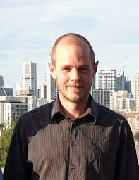 Zachreson Cameron合作论文数2
 Igor Aharonovich合作论文数School of Mathematical and Physical Sciences, Faculty of Science, University of Technology Sydney;Writeitupnow2Bresin Matthew合作论文数2Bahm Alan合作论文数2
 Chad Rue合作论文数FEI Company2david h narum合作论文数1mark w utlaut合作论文数1Lukas Eriksson合作论文数1Alpcan Önür合作论文数1Cedric Bouchet-Marquis合作论文数1Paul Fremdling合作论文数1Leon Van Kouwen合作论文数1Evan Raeker合作论文数1
 Jenna Schardt合作论文数1Dinesh K Chinthapalli合作论文数1Jan Böhning合作论文数Sir William Dunn School of Pathology, University of Oxford1
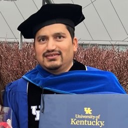 Amrit P. Kaphle合作论文数Dept Phys & Astron, Univ Kentucky1
 R. N. Gannon合作论文数Dept Chem, Univ Oregon1B. L. Thiel合作论文数College of Nanoscale Science and Engineering, SUNY Polytechnic Institute1
 William C. Lenthe合作论文数Department of Materials Science and Engineering, University of California Santa Barbara1
 Joseph Gault合作论文数Univ Oxford, Dept Chem, Oxford, England1Qian Wu合作论文数1Sarah K Lami合作论文数1
 Nicolas J. Briot合作论文数Chemical and Materials, University of Kentucky1
 Alessandro Mottura合作论文数School of Metallurgy and Materials, College of Engineering and Physical Sciences, University of Birmingham1Randolph Sophia合作论文数1
 Tanmay Bharat合作论文数Sir William Dunn School of Pathology, University of Oxford1
 Albert Konijnenberg合作论文数1
 Esser Tim K合作论文数Wilhelm-Ostwald-Institut für Physikalische und Theoretische Chemie, Universität Leipzig1
 Justin Benesch合作论文数Department of Chemistry, University of Oxford;Benesch Group, Kavli Institute for NanoScience Discovery, University of Oxford1




