For in-situ analysis, the capability to capture data at high speed and dose efficiency is critical for capturing data over the desired range of in-situ conditions.Single electron counting direct detection cameras are the ideal detector choice for in-situ (scanning) transmission electron microscopy due to their inherently high detective quantum efficiency (DQE) and high frame rates [1].Furthermore, the rejection of read noise by such detectors, allows collection of a large number of in-situ frames, which can then be summed together as needed to balance signal-to-noise against temporal resolution during data analysis.A prototype method for in-situ spectrum image (SI) acquisition was recently demonstrated using a current generation EELS spectrometer (GIF Continuum) and Gatan DigitalMicrograph [2].Copper (II) oxide was reduced in-situ by heating in a MEMS based heating holder (Wildfire, DENSSolutions).ELNES mapping of Cu L 2,3 spectra performed both live and postacquisition showed a trend of decreasing Cu oxidation state from majority Cu(II) to Cu(0) at the end of the experiment alongside spontaneous changes in CuO particle morphology at specific temperatures.Limitations in the prototype approach were also observed.Non-zero dead time between successive spectrum image passes was found to account for a large fraction of total acquisition time if the time to acquire each SI pass was short.A requirement to keep the full SI time series in system memory limited the temperature range and increment that could be used.Finally, a lack of native software features for processing SI time series data made processing times impractical for larger datasets including multiple ionization edges.Here we demonstrate recent advances in in-situ spectrum imaging capability that have been made possible by a flexible next generation scan control system (Digiscan3) and an expansion of the in-situ software features in DigitalMicrograph.Continuous multiple pass scanning can now be performed, allowing successive spectrum image passes to be acquired with zero dead time between scans.Hardware synchronized sub-pixel scanning can also be performed, giving an increase in scan speed of up to 90x that of the previous generation scan system.These features combined, dramatically increase the time resolution at which in-situ spectrum image acquisition can be performed.New software features include full support of all SI processing functions for in-situ, allowing rapid data analysis.Finally, all SI data acquired is now streamed to disk by the software, drastically increasing the size of datasets that may be captured.In-situ heating has been performed on a variety of materials including: metal nanoparticles, and oxide nanopowders such as Fe 2 O 3 .H 2 O as shown in figure 1. Heating cycles were performed both with and without holder synchronization and control.The benefits of both approaches are discussed.To explore a more complex experimental setup, the ferroic phase changes of improper ferroelectric Cu, Cl, and Fe, I based boracites were investigated by in-situ heating and cryogenic cooling.Changes in the fine structure of the Cu, and Fe with corresponding O were analyzed at the ferroelectric domain walls during temperature induced phases changes and when moved by an applied bias.As the transition metal coordination chemistry dictates the resulting functionality (i.e.charge or magnetism) it is essential to be able to analyse the EELS fine structure during domain wall dynamics.
Journal Article Continuous 4D STEM Recording and Visualization for In-situ Experiments Get access Benjamin K Miller, Benjamin K Miller Gatan, IncPleasanton, CA, United States Corresponding author: Benjamin.Miller@ametek.com Search for other works by this author on: Oxford Academic Google Scholar Bernhard Schaffer, Bernhard Schaffer Gatan, IncPleasanton, CA, United States Search for other works by this author on: Oxford Academic Google Scholar Anahita Pakzad Anahita Pakzad Gatan, IncPleasanton, CA, United States Search for other works by this author on: Oxford Academic Google Scholar Microscopy and Microanalysis, Volume 29, Issue Supplement_1, 1 August 2023, Page 271, https://doi.org/10.1093/micmic/ozad067.123 Published: 22 July 2023
Journal Article Autonomous Multimodal Spectrum Imaging for High Throughput Data Acquisition Get access Liam Spillane, Liam Spillane Gatan Inc., Pleasanton, CA, United States Corresponding author: liam.spillane@ametek.com Search for other works by this author on: Oxford Academic Google Scholar Bernhard Schaffer, Bernhard Schaffer Gatan Inc., Pleasanton, CA, United States Search for other works by this author on: Oxford Academic Google Scholar Paul J Thomas, Paul J Thomas Gatan Inc., Pleasanton, CA, United States Search for other works by this author on: Oxford Academic Google Scholar Michael Zachman Michael Zachman Center for Nanophase Materials Science, Oak Ridge National Laboratory, Oak Ridge, TN, United States Search for other works by this author on: Oxford Academic Google Scholar Microscopy and Microanalysis, Volume 29, Issue Supplement_1, 1 August 2023, Pages 1902–1903, https://doi.org/10.1093/micmic/ozad067.982 Published: 22 July 2023
Journal Article Automated Spectrum Imaging Using Hybridized DMScript and Python Code in DigitalMicrograph Get access Liam Spillane, Liam Spillane Gatan Inc., Pleasanton, CA Corresponding author: liam.spillane@ametek.com Search for other works by this author on: Oxford Academic Google Scholar Bernhard Schaffer Bernhard Schaffer Gatan Inc., Pleasanton, CA Search for other works by this author on: Oxford Academic Google Scholar Microscopy and Microanalysis, Volume 28, Issue S1, 1 August 2022, Pages 2922–2923, https://doi.org/10.1017/S1431927622010960 Published: 01 August 2022
Modern electron microscopy can generate large amounts of data. While this may reveal details of the sample in unprecedented detail, collecting more data can also obscure what’s most important. In-situ experiments where data is acquired continuously further increase the data volume. In-situ experiments may also require the user to make decisions about what to do next based on the changes observed in the microscope. However, depending on the sample and the software setup, these changes are not always obvious from a default live view of the data displayed in real-time. Given the large data volume, enhanced flexibility to process and visualize data in a variety of ways is valuable, especially if this can be done in real-time to understand the changes occurring to the sample. This enables informed decision making during the experiment, increasing the chances that valuable data is collected.
An abstract is not available for this content so a preview has been provided. As you have access to this content, a full PDF is available via the ‘Save PDF’ action button.
During in-situ experiments it is often important for the user to make good decisions about what to do next. Should the in-situ conditions be changed, or should the data collection frequency and details be modified? Has the sample been transformed during the experiment, or destroyed, or is it unchanged? In some cases, a simple visual inspection of the live 2D image is sufficient to answer these questions and make good decisions. In other cases, the decision is not so straightforward, and some processing is required before the user can draw any conclusions. Commercial software can already do some processing to transform the raw sensor output into “clean” data, or to produce a live FFT. However, new data acquisition and processing methods are constantly being developed, and often the built-in live processing in commercial software does not yet support these advances. Gatan Microscopy Suite (GMS) has always had scripting capabilities which can be used to customize live processing, and recently Python scripting has been added, making this more accessible to the larger community. In this work we demonstrate real-time Python processing of both 4D STEM datasets and high-resolution images to map the spatial distribution of crystallinity during acquisition. It is inherently difficult to see anything in the raw data of a series of 4D STEM datasets due to the dimensionality, which prohibits direct display on a 2D monitor. It can also become difficult to see the crystallinity of a material over a large field of view because modern cameras, like the K3 IS used to collect this data, produce images that are too large to display on most monitors. The methodology for this live Python-based processing is shown in Figure 1. In the case of 4D STEM, each diffraction pattern is processed to find the maximum intensity pixel, while masking a user-defined central region of the pattern. The direction from the pattern center, spacing, and intensity of this maximum point are determined, and color maps are produced. The hue can be either the angle or distance from center while the brightness of the color is determined by the intensity. A 2D color map is thus generated from each 4D data cube. If a series of data cubes is acquired, a map can be generated for each one, resulting in a color video. This approach can be extended for processing large high resolution TEM images. First a grid of overlapping windows is extracted from a single large 2D image, and the FFT of each window is computed. These FFTs are placed into a 4D cube which is analogous to that generated using 4D STEM, but with diffractograms instead of diffraction patterns. This 4D cube of FFTs can then be analyzed in the same way as a 4D STEM data cube. This processing has been applied during video recording of Sn nanoparticle melting and recrystallization, where the temperature was oscillated between 50 and 300 °C. Maps processed after acquisition are shown in Figure 2, and screenshot videos of live processing during acquisition will be shown in my talk. While it was not obvious from the raw video that the nanoparticles re-crystallize in different orientations each time, this is clear from the maps. Figures 1 and 2 primarily demonstrate the parallels and similarities between the 4D STEM and HR TEM based approaches. However, there are differences and tradeoffs which would make one or the other optimal for a given experiment. The primary benefit of the FFT-based approach is the potential for capturing data with the high temporal resolution afforded by TEM and modern in-situ cameras. The diffractogram data is also easier to process since the center of the pattern is always in the exact center of the image. However, the spatial resolution of the FFT-based maps tends to be poor and the volume of reciprocal space that is covered is usually less than with 4D STEM. Finally, the FFT approach is better
We outline a simple routine to correct for non-uniformities in the energy dispersion of a post-column electron energy-loss spectrometer for use in scanning transmission electron microscopy. We directly measure the dispersion and its variations by sweeping a spectral feature across the full camera to produce a calibration that can be used to linearize datasets post-acquisition, without the need for reference materials. The improvements are illustrated using core excitation electron energy-loss spectroscopy (EELS) spectra collected from NiO and diamond samples. The calibration is rapid and will be of use in all EELS analysis, particularly in assessments of the chemical states of materials via the chemical shift of core-loss excitations.
Electron energy-loss spectroscopy (EELS) performed in the scanning transmission electron microscope (STEM) is a powerful technique for probing local electronic structure at high spatial resolution via the spectrum imaging (SI) paradigm. For in-situ analysis, the capability to capture spectral data at both high speed and high dose efficiency is critical. Traditional CCD based detectors used for EELS are capable of high spectral rates but give inherently low collection efficiency at high speed due to fixed readout dead time. Spectral quality is further compromised by the need to perform high levels of asymmetric binning to achieve the maximum frame rate. The current generation of CMOS based EELS detectors do not rely on binning for performance gains and utilize rolling shutter readout. With the use of fast electrostatic deflectors, these detectors can achieve nearly 100% live time readout at high spectral rates ( > 8 kHz) giving high dose efficiency. Incorporating such a detector into an optimized STEM EELS acquisition system gives a highly efficient platform for in-situ STEM EELS experiments.
We investigated the structure of the tungsten bronze barium neodymium titanates Ba(6-3n)Nd(8+2n)Ti(18)O(54), which are exploited as microwave dielectric ceramics. They form a complex nanostructure, which resembles a nanofilm with stacking layers of ∼12 Å thickness. The synthesized samples of Ba(6-3n)Nd(8+2n)Ti(18)O(54) (n = 0, 0.3, 0.4, 0.5) are characterized by pentagonal and tetragonal columns, where the A cations are distributed in three symmetrically inequivalent sites. Synchrotron X-ray diffraction and electron energy loss spectroscopy allowed for quantitative analysis of the site occupancy, which determines the defect distribution. This is corroborated by density functional theory calculations. Pentagonal columns are dominated by Ba, and tetragonal columns are dominated by Nd, although specific Nd sites exhibit significant concentrations of Ba. The data indicated significant elongation of the Ba columns in the pentagonal positions and of the Nd columns in tetragonal positions involving a zigzag arrangement of atoms along the b lattice direction. We found that the preferred Ba substitution occurs at Nd[3]/[4] followed by Nd[2] and Nd[1]/[5] sites, which is significantly different to that proposed in earlier studies. Our results on the Ba(6-3n)Nd(8+2n)Ti(18)O(54) "perovskite" superstructure and its defect distribution are particularly valuable in those applications where the optimization of material properties of oxides is imperative; these include not only microwave ceramics but also thermoelectric materials, where the nanostructure and the distribution of the dopants will reduce the thermal conductivity.
Journal Article Absence of phase separation in nano-chessboard super-lattices in A-site deficient Ca-stabilized Nd2/3TiO3 Get access Feridoon Azough, Feridoon Azough School of Materials, Materials Science Centre, University of Manchester, Manchester M1 7HS, United Kindgom Search for other works by this author on: Oxford Academic Google Scholar Demie Kepaptsoglou, Demie Kepaptsoglou SuperSTEM Laboratory, STFC Daresbury Campus, Keckwick Lane, Warrington WA4 4AD, United Kingdom Search for other works by this author on: Oxford Academic Google Scholar Quentin M Ramasse, Quentin M Ramasse SuperSTEM Laboratory, STFC Daresbury Campus, Keckwick Lane, Warrington WA4 4AD, United Kingdom Search for other works by this author on: Oxford Academic Google Scholar Bernhard Schaffer, Bernhard Schaffer SuperSTEM Laboratory, STFC Daresbury Campus, Keckwick Lane, Warrington WA4 4AD, United Kingdom Search for other works by this author on: Oxford Academic Google Scholar Robert Freer Robert Freer School of Materials, Materials Science Centre, University of Manchester, Manchester M1 7HS, United Kindgom Search for other works by this author on: Oxford Academic Google Scholar Microscopy and Microanalysis, Volume 21, Issue S3, 1 August 2015, Pages 1353–1354, https://doi.org/10.1017/S1431927615007552 Published: 23 September 2015
In this work, a novel high precision local positioning system is presented. The system is capable of determining the two- or three-dimensional position of a localization unit relative to a set of wireless active transponders, which are mounted at defined anchor positions in a range of up to 200 meters. Operating in the 2.4 GHz ISM band at a bandwidth of approximately 60 MHz, the localization unit carries out distance measurements to the transponders and then calculates its own position in space by the use of a multilateration algorithm. The ranging measurements are based on a cooperative roundtrip time of flight estimation, using amplitude modulated pseudo-noise sequences for pulse compression and a time division multiple access scheme to support multiple transponders in a single measurement cycle. In contrast to multilateration systems based on the time difference of arrival, our roundtrip time of flight system does not need synchronization by wires or fibers between the anchor nodes. This makes setup and operation as easy as placing the transponders and their power supply at precisely known positions in the field. In this paper, the system setup and the used algorithms are described, and an evaluation of the performance is given from outdoor field tests, comparing the position estimates to those of a commercial differential GPS system with inertial sensor support. The raw, untracked positioning results show an accuracy in the decimeter region with seven anchor transponders in a field of 180 x 200 meters.
An abstract is not available for this content so a preview has been provided. As you have access to this content, a full PDF is available via the ‘Save PDF’ action button.
Stepped antiphase boundaries are frequently observed in Ti-doped Bi0.85Nd0.15FeO3, related to the novel planar antiphase boundaries reported recently. The atomic structure and chemistry of these steps are determined by a combination of high angle annular dark field and bright field scanning transmission electron microscopy imaging, together with electron energy loss spectroscopy. The core of these steps is found to consist of 4 edge-sharing FeO6 octahedra. The structure is confirmed by image simulations using a frozen phonon multislice approach. The steps are also found to be negatively charged and, like the planar boundaries studied previously, result in polarisation of the surrounding perovskite matrix.
Radar systems using stepped frequency signals that are uniformly shifted through a certain band require a high amount of spectrum and also suffer from long data acquisition times needed to provide high resolution and a huge unambiguity range at the same time. In order to break up the limitations in the performance of such a radar system, a nonuniform spacing of frequency steps is described, that allows increasing the update rate as well as reducing the amount of spectrum while retaining multipath resolution and the area that can be unambiguously covered. Similarly, the proposed signal design can also be used to provide an enhanced resolution capability without increasing measurement time and bandwidth utilization. Both can be achieved by the use of certain step patterns including several gaps but allowing for full augmentation of the missing data. In addition to the signal design scheme, a method for the signal processing of the data is described that can be used to achieve a sidelobe level similar to the one obtained when using a conventional uniform pattern utilizing the full amount of bandwidth. In addition to Monte Carlo simulations, the effectiveness of the scheme is proven by laboratory measurements.
Nanometric bubbles filled with nitrogen, located adjacent to FenN (n = 3 or 4) nanocrystals with in (Ga,Fe)N layers, are identified and characterized using scanning transmission electron microscopy (STEM) and electron energy-loss spectroscopy (EELS). High-resolution STEM images reveal a truncation of the Fe-N nanocrystals at their boundaries with the nitrogen bubbles. A controlled electron beam hole drilling experiment is used to release nitrogen gas from a bubble in situ in the electron microscope. The density of nitrogen in an individual bubble is measured to be 1.4 ± 0.3 g/cm. These observations provide an explanation for the location of surplus nitrogen in the (Ga,Fe)N layers which is liberated by the nucleation of FenN (n> 1) nanocrystals during the growth.
High quality ceramics of Ba((Co0.7Zn0.3)1/3Nb2/3)O3 (BCZN), Ba(Mg1/3Nb2/3)O3 (BMN) and Ba(Mg1/3Ta2/3)O3 (BMT) were prepared by the mixed oxide route using sintering temperatures up to 1620°C. Products with a high degree of cation ordering exhibited dielectric Q×f values from 83,000GHz (BCZN) to 360,000GHz (BMT). High Resolution TEM and aberration-corrected scanning transmission electron microscopy (STEM) revealed ordering domains and type I, II and III boundary structures. High-Angle Angular Dark Field (HAADF) STEM images provided direct evidence of 1:2 ordering and stacking sequences, and the presence of disordered regions within domain boundaries. The exceptionally high Q×f values for BMT are associated with a high degree of B-site ordering and the removal of domain boundaries in large, single domain grains. The catastrophic degradation of Q×f values in BMN after prolonged sintering is associated with formation of a lossy ferroelectric secondary phase (Ba3Nb2O8), and changes to composition and stoichiometry of BMN grains.
 Gerald Kothleitner合作论文数36
 Ferdinand Hofer合作论文数Institute of Physical and Theoretical Chemistry, Graz University of Technology/Institute of Electron Microscopy and Nanoanalysis, Graz University of Technology/Anton Paar GmbH35
 Werner Grogger合作论文数Institute of Electron Microscopy and Nanoanalysis, Graz University of Technology;Institute of Solid State Physics, Graz University of Technology33
 Quentin Ramasse合作论文数School of Chemical and Process Engineering, Faculty of Engineering and Physical Sciences, University of Leeds;School of Physics and Astronomy, , Faculty of Engineering and Physical Sciences, University of Leeds;SuperSTEM Laboratory, EPSRC National Research Facility for Advanced Electron Microscopy10
 Ian Maclaren合作论文数School of Physics and Astronomy, University of Glasgow10A. J. Craven合作论文数9Miroslava Schaffer合作论文数Dept Mol Struct Biol, Max Planck Inst Biochem8Liam Spillane合作论文数7Feridoon Azough合作论文数7
 Benjamin K. Miller合作论文数6Gerrit Kalverkamp合作论文数6
 Robert Freer合作论文数Department of Materials, University of Manchester6
 Erwin Biebl合作论文数Department of Electrical and Computer Engineering, Technische Universitat Munchen6
 Daniel Abou-Ras合作论文数Helmholtz-Zentrum Berlin für Materialien und Energie;Technical University of Berlin6Sebastian S. Schmidt合作论文数5
 Paul Thomas合作论文数5
 Raquel Caballero合作论文数Department of Applied Physics, Universidad Autónoma de Madrid5
 Kambiz Kalantari合作论文数4Wang LiQiu合作论文数4Ray D. Twesten合作论文数University of Illinois Materials Research Laboratory4Alan J. Craven合作论文数4
 Michael Sarahan合作论文数Chemistry and Materials Science Department, University of California4Anahita Pakzad合作论文数3s miao合作论文数3Christoph Mitterbauer合作论文数3
 Christoph Koch (KOCH C T)合作论文数Humboldt Univ3
 Andras Kovacs合作论文数Forschungszentrum Julich, Ernst Ruska Ctr Microscopy & Spect Electrons, D-52425 Julich, Germany3
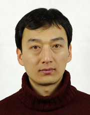 Shu Miao (苗澍)合作论文数Dalian Institute of Chemical Physics, Chinese Academy of Sciences;JEOL3
 Demie Kepaptsoglou合作论文数SuperSTEM Laboratory, Science &Technology Facilities Council Daresbury Laboratories;SuperSTEM Laboratory, Science & Technology Facilities Council Daresbury Laboratories, Daresbury WA4 4AD, United Kingdom;3
 Egbert Zojer合作论文数Graz University of Technology, Technische Universität Graz3
 Ian Reaney合作论文数Department of Materials Science and Engineering, University of Sheffield3K. Riegler合作论文数3
 Mario Sergio Moreno合作论文数Organic Chemistry Department, Cordoba University3Jürgen O. Besenhard合作论文数3
 Rafal Dunin-Borkowski合作论文数Ernst Ruska-Centrum für Mikroskopie und Spektroskopie mit Elektronen, Forschungszentrum Jülich GmbH;Institute for Microstructure Research, Forschungszentrum Jülich GmbH;RWTH Aachen University3Alexander Pogantsch合作论文数3
 Thomas Unold合作论文数Department Structure and Dynamics of Energy Materials, Helmholtz-Zentrum Berlin3L. Q. Wang合作论文数2Andreas Schertel合作论文数2Kasim Sader合作论文数Thermo Fisher Sci, Mat & Struct Anal, Achtseweg Noord 5, NL-5651 GG Eindhoven, Netherlands2
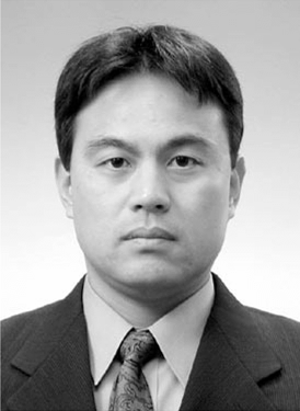 Shimada Takeshi合作论文数2
 Hans-Werner Schock合作论文数Consultant PV Technologies;Institute of Technology, Helmholtz-Zentrum Berlin2Sterianou Iasmi合作论文数2Cory Czarnik合作论文数2
 Kannan M. Krishnan合作论文数Department of Materials Science & Engineering, College of Engineering, University of Washington2
 Tomasz Dietl合作论文数International Research Centre MagTop, Institute of Physics, Polish Academy of Sciences2
 Angelika Basch合作论文数Ian Wark Research Institute, University of South Australia2
 Pyuck-Pa Choi合作论文数Nanostructured Materials & Advanced Characterization Laboratory, Department of Materials Science and Engineering, Korea Advanced Institute of Science and Technology2
 Joerg R. Jinschek合作论文数National Centre for Nano Fabrication and Characterization, Technical University of Denmark2




