Single nuclear spins in silicon are a promising resource for quantum technologies due to their long coherence times and excellent control fidelities. Qubits and qudits have been encoded on donor nuclei, with successful demonstrations of Bell states and quantum memories on the spin- / 2 1 P 31 and cat-qubits on the spin- / 2 7 Sb 123 nuclei. Isoelectronic nuclear spins coupled to gate-defined quantum dots, such as the naturally occurring Si 29 isotope, possess no additional charge and allow for the coupled electron to be shuttled without destroying the nuclear spin coherence. Here, we demonstrate the coupling of a spin- / 2 9 Ge 73 nuclear spin to a gate-defined quantum dot in SiMOS via Pauli spin blockade readout using rf reflectometry. We observe the hyperfine interaction (HFI) to the coupled quantum dot electron and are able to tune it from 180 to 350 kHz, through the voltages applied to the lateral gate electrodes. This smaller HFI combined with the faster readout enable easier quantum nondemolition readout of the nuclear spin state. Thus, this work lays the foundation for future spin control experiments on the spin- / 2 9 qudit as well as more advanced experiments such as entanglement distribution between distant nuclear spins or repeated weak measurements.
Emerging quantum technologies based on the nitrogen-vacancy (NV) centre in diamond require carefully engineered material with controlled defect density, optimised NV formation processes, and minimal crystal strain. The choice of NV generation technique plays a crucial role in determining the quality and performance of these centres. In this work, we investigate NV centre formation in nitrogen-doped diamond using femtosecond (fs) laser processing. We systematically examine the effect of laser pulse energy on NV production and quality using photoluminescence and optically detected magnetic resonance measurements. We also probe the role of pre-existing lattice defects formed by electron irradiation and consider defect evolution over extended dwell times. Finally, we are able to identify a regime where the main action of the fs-laser is to diffuse rather than create vacancies. This local annealing capability expands the toolkit for tailored NV production and presents opportunities for fine tuning defect populations.
Spins in silicon that are accessible via a telecom-compatible optical transition are a versatile platform for quantum information processing that can leverage the well-established silicon nanofabrication industry. Key to these applications are long coherence times on the optical and spin transitions to provide a robust system for interfacing photonic and spin qubits. Here, we report telecom-compatible Er3+ sites with long optical and electron spin coherence times, measured within a nuclear spin-free silicon crystal (<0.01
Atomic-size defects, known as color centers, hosted in solid-state materials, such as silicon carbide and diamond, are promising candidates for integration into chip-scale quantum systems. Specifically, the incorporation of these color centers within photonic integrated circuits may enable precise control over their inherent photophysical properties through strong light-matter interaction. Here, we investigate ion-implanted erbium (Er3+) defects embedded in nanometric thin-film 4H-silicon-carbide-on-insulator (4H-SiCOI). Optimized implantation conditions and thermal annealing processes designed to enhance the photoluminescence excitation (PLE) emission characteristics of the Er3+ defect are reported. By examining key properties such as photoluminescence intensity, optical lifetime, and polarization, we present an analysis of ensemble Er3+ defects within 4H-SiCOI, providing insights into their potential for future quantum applications.
Optically addressable solid-state spins have been proposed as robust radiofrequency (RF)-optical transducers sensitive to a specific RF frequency tuned by external magnetic fields but often require precise field alignment with the system's symmetry axis. Here we introduce an isotropic solid-state spin system, namely, weakly coupled spin pairs in hexagonal boron nitride, which acts as an RF-optical transducer independent of the direction of the tuning magnetic field. Using this platform, we demonstrate a single-frequency RF receiver with frequency tunability from 0.1 to 19 GHz and an instantaneous wideband RF spectrum analyzer by applying a magnetic field gradient to encode RF frequency into spatial position. We utilize the spectrum analyzer to detect free-space-transmitted RF signals matching the strength and frequency of typical Wi-Fi signals. This work exemplifies the unique capabilities of isotropic spins to operate as RF sensors, while circumventing the challenging requirement of precisely aligned magnetic fields facing conventional solid-state spins.
Vanadium silicide, V3Si, is a promising superconductor for silicon-based superconducting (SC) devices due to its compatibility with silicon substrates and its potential for integration into existing semiconductor technologies. However, to date there have been only a limited number of studies of the formation of SC V3Si thin films and the associated structural and superconducting properties. This work aims to explore the structural characteristics and SC properties of V3Si films, paving the way for the development of functional SC devices for quantum technology applications. We have investigated the formation of V3Si films by directly depositing vanadium (V) onto thermally grown SiO2 on Si, followed by high-vacuum annealing to induce the phase transformation into V3Si. Rutherford Backscattering Spectrometry (RBS) was employed throughout the sample growth process to analyze the material composition as a function of depth using a He-4(+) ion beam. Analysis of the RBS data confirmed that the V layer fully reacted with the SiO2 substrate to form V3Si at the interface, in addition to a vanadium oxide (VOx) layer forming atop the V3Si film. The thickness of the V3Si layer ranges from 63 to 130 nm, with annealing temperatures between 750 degrees C and 800 degrees C. A sharp SC transition was observed at T-c = 13 K in the sample annealed at 750 degrees C, with a narrow transition width (Delta T-c)of0.6 K. Initial reactive ion etching (RIE) studies yielded promising results for local removal of the (VOx) to facilitate electrical contact formation to the SC layer.
Diamonds containing nitrogen-valency (NV) centers are an important emerging material for applications involving local environment sensing. The nature of these doped diamonds allows for the development of magnetic field sensing technologies, with responses that are quantifiable and sensitive to weak signals. The incorporation of these diamonds within optical fibers allows for a direct approach in the design and fabrication of a compact and effective sensing device. We investigated the inclusion of NV-doped micron-sized diamonds within silicate glass fibers by way of filament fusion splicing, such that a single diamond particle is embedded within the cross-sectional interface between spliced fibers, termed the splice-point. The inclusion of a single diamond crystal establishes a mono- crystalline structure in which the NV centers reside and can operate, allowing for vector magnetic field sensing opportunities. The process developed involves adhering a single diamond particle of similar to 50 mu m size to the end of a cleaved fiber, ready for splicing. A Vytran fusion splicer was used to perform the splicing procedure, where the cleaved ends of the diamondtipped and bare fibers become fused by heating and pushing the ends of the fibers together; the result is a diamond embedded at the splice-point. After the embedding process, the NV centers were excited with a 532 nm laser. Photoluminescence from these NV centers was guided through the fiber and coupled into an HR550 series Horiba spectrometer. The measured fluorescence spectrum at 600-800 nm (zero-phonon line at 640 nm) showed the typical spectral shape of the NV fluorescence, indicating the preservation of the diamond particle and NV centers during the thermal treatment of the splicing process.
Isotopically enriched silicon (Si) can greatly enhance qubit coherence times by minimizing naturally occurring $^{29}$Si which has a non-zero nuclear spin. Ultra-high fluence $^{28}$Si ion implantation of bulk natural Si substrates was recently demonstrated as an attractive technique to ultra-high $^{28}$Si isotopic purity. In this work, we apply this $^{28}$Si enrichment process to produce $^{28}$Si and $^{28}$Si-on-insulator (SOI) samples. Experimentally, we produced a $^{28}$Si sample on natural Si substrate with $^{29}$Si depleted to 7~ppm (limited by measurement noise floor), that is at least 100 nm thick. This is achieved with an ion energy that results in a sputter yield of less than one and an ultra-high ion fluence, as supported by our improved computational model that is based on fitting a large number of experiments. Further, our model predicts the $^{29}$Si and $^{30}$Si depletion in our sample to be less than 1~ppm. In the case of SOI, ion implantation conditions are found to be more stringent than those of bulk natural Si in terms of minimizing threading dislocations upon subsequent solid phase epitaxy annealing. Finally, we do not observe open volume defects in our $^{28}$SOI and $^{28}$Si samples after SPE annealing (620°C, 10 minutes).
The negatively charged Nitrogen-vacancy (NV-) color center in diamond is widely studied because of numerous applications of this unique quantum system in sensing and quantum information sciences. While substitutional nitrogen is required to form NV- centers, it also yields other paramagnetic defects - primarily the neutrally charged substitutional nitrogen centers (P1) - that decrease NV- spin coherence which in turn degrades performance in applications. Herein, we investigate high-pressure high-temperature synthesized diamond microparticles (ca. 140-185 μm) having lower - ranging from 3 to 38 ppm - than the typical nitrogen content of type 1b diamond (ca. 100 ppm and higher) typically used for production of fluorescent diamond particles with NV- centers. A suite of electron paramagnetic resonance, optically detected magnetic resonance, and nuclear magnetic resonance methods are used to characterize spin properties of P1 and NV- centers in the particles. Upon decreasing the nitrogen content from 29 ppm to 3 ppm, the ensemble NV- T 2 relaxation time increased by about 3-fold as measured directly in the Hahn Echo experiment at 1.2 Tesla. Analysis of electronic relaxation of P1 centers revealed the existence of at least two distinct populations of P1 centers, consisting of fast and slower relaxing spins. Even with <10 ppm nitrogen contents, the analysis indicated a highly heterogenous distribution of P1 centers, suggesting the possibility of P1 spin clustering in even at low concentrations. The combined data demonstrate that the particles prepared from HPHT diamond with a low nitrogen content offer improved spin properties that are beneficial for NV- sensing applications.
Controlled bandgap modulation is of particular interest for next generation optoelectronic devices, allowing the development of 'active' or 'reconfigurable' detectors and emitters. In van der Waals layered semiconductors, which exhibit high strain tolerance, strain has become a notable tool for active bandgap tuning. In this work, we demonstrate a flexible bulk InSe gated photoconductor with strain-induced modulation of the bandgap energy, shifting to higher and lower energies under compression and tension, respectively. Photoluminescence measurements reveal shift rates of around 117.1 meV·%-1 in tension and 107.6 meV·%-1 in compression. Spectral responsivity measurements indicate smaller shift rates, likely due to nonuniform strain application. Notably, these flexible devices achieve impressive performance with specific detectivities up to 3.78 × 1012 cm·Hz1/2·W-1, a rise time of 4.1 μs, and a responsivity of 1.25 × 10³ A·W-1. The realization of high responsivity and fast response times underscores the potential of this device architecture for advanced optoelectronic applications.
The nitrogen‐vacancy (NV) center is a photoluminescent defect in diamond that exists in different charge states, NV ‐ and NV 0 , that are sensitive to the NV's nanoscale environment. Here, all‐optical voltage sensing with NV centers in fluorescent nanodiamonds (FNDs) is demonstrated in a solid‐state device based on electric field‐induced NV charge state modulation. More than 95% of FNDs integrated into a polymer‐based capacitor device show a transient increase in NV − PL intensity up to 31% within 0.1 ms after application of an external voltage, accompanied by a simultaneous decrease in NV 0 PL. The NV − PL signal increases with increasing electric field from 0 to 619 kV cm −1 . The best electric field sensitivity for a single FND is 18 V cm −1 Hz −½ . The NV charge state photodynamics are investigated on the millisecond timescale. The change in NV PL is found to strongly depend on the rate of photoexcitation. A model is proposed that qualitatively explains the results based on an electric field‐induced redistribution of photoexcited electrons from substitutional nitrogen to NV centers, leading to a transient conversion of NV 0 to NV − centers. These results contribute to the development of FNDs as reliable, all‐optical, nanoscale electric field sensors in solid‐state systems.
The use of nuclear spins for quantum computation is limited by the difficulty in creating genuine quantum entanglement between distant nuclei. Current demonstrations of nuclear entanglement in semiconductors rely on coupling the nuclei to a common electron, which is not a scalable strategy. In this work, we demonstrated a two-qubit controlled-Z logic operation between the nuclei of two phosphorus atoms in a silicon device, separated by up to 20 nanometers. Each atom binds separate electrons, whose exchange interaction mediates the nuclear two-qubit gate. We prepared and measured a nuclear Bell state with a fidelity of [Formula: see text] and a concurrence of [Formula: see text]. With this method, future progress in scaling up semiconductor spin qubits can be extended to the development of nuclear spin-based quantum computers.
The realization of a quantum computer represents a tremendous scientific and technological challenge due to the extreme fragility of quantum information. The physical support of information, namely the quantum bit or qubit, must at the same time be strongly coupled to other qubits by gates to compute information, and well decoupled from its environment to keep its quantum behavior. An interesting physical system for realizing such qubits are magnetic impurities in semiconductors, such as bismuth donors in silicon. Indeed, spins associated to bismuth donors can reach an extremely long coherence time -- of the order of seconds. Yet it is extremely difficult to establish and control efficient gates between these spins. Here we demonstrate a protocol where single bismuth donors can coherently transfer their quantum information to a superconducting flux qubit, which acts as a mediator or quantum bus. This superconducting device allows to connect distant spins on-demand with little impact on their coherent behavior.
Diamond-embedded optical fibers with negatively charged nitrogen-vacancy (NV)centers have great potential for remote and distributed magnetic field sensing. However, themagnetic field sensitivity of the currently proposed fiber configuration is limited. This work usesa numerical approach to investigate the effect of structured diamonds on enhancing the excitationand collection efficiency in an optical fiber through a hybrid modelling approach. The resultsrevealed that a 690-times enhancement is achievable with a pillar-shaped diamond embedded ina fiber (c) 2024 Optica Publishing Group under the terms of the Optica Open Access Publishing Agreement
Characterising charge transport in a material is central to the understanding of its electrical properties, and can usually only be inferred from bulk measurements of derived quantities such as current flow. Establishing connections between host material impurities and transport properties in emerging electronics materials, such as wide bandgap semiconductors, demands new diagnostic methods tailored to these unique systems, and the presence of optically-active defect centers in these materials offers a non-perturbative, in-situ characterisation system. Here, we combine charge-state sensitive optical microscopy and photoelectric detection of nitrogen-vacancy (NV) centres to directly image the flow of charge carriers inside a diamond optoelectronic device, in 3D and with temporal resolution. We optically control the charge state of background impurities inside the diamond on-demand, resulting in drastically different current flow such as filamentary channels nucleating from specific, defective regions of the device. We then optically engineered conducting channels that control carrier flow, key steps towards optically reconfigurable, wide bandgap designer optoelectronics. We anticipate our approach might be extended to probe other wide-bandgap semiconductors (SiC, GaN) relevant to present and emerging electronic technologies.
This study explores the optimisation of a diamond pillar geometry with NV centres near the tip. Modelling incoherent fluorescence emission from NV ensembles, we achieve fivefold backward directional emission over forward. (C) 2024 The Author(s)
Masers once represented the state-of-the-art in low noise microwave amplification technology, but eventually became obsolete due to their need for cryogenic cooling. Masers based on solid-state spin systems perform most effectively as amplifiers, since they provide a large density of spins and can therefore operate at relatively high powers. Whilst solid-state masers oscillators have been demonstrated at room temperature, continuous-wave amplification in these systems has only ever been realized at cryogenic temperatures. Here we report on a continuous-wave solid-state maser amplifier operating at room temperature. We achieve this feat using a practical setup that includes an ensemble of nitrogen-vacancy center spins in a diamond crystal, a strong permanent magnet and simple laser diode. We describe important amplifier characteristics including gain, bandwidth, compression power and noise temperature and discuss the prospects of realizing a room-temperature near-quantum-noise-limited amplifier with this system. Finally, we show that in a different mode of operation the spins can be used to cool the system noise in an external circuit to cryogenic levels, all without the requirement for physical cooling.
A gallium interstitial defect is thought to be responsible for the spectacular spin-dependent recombination in GaAs_{1-x}N_{x} dilute nitrides. Current understanding associates this defect with at least two in-gap levels corresponding to the (+/0) and (++/+) charge-state transitions. Using a spin-sensitive photoinduced current transient spectroscopy, the in-gap electronic structure of a x=0.021 alloy is revealed. The (+/0) state lies ≈0.27 eV below the conduction band edge, and an anomalous, negative activation energy reveals the presence of not one but two other in-gap states. The observations are consistent with a (++/+) state ≈0.19 eV above the valence band edge, and a (+++/++) state ≈25 meV above the valence band edge.
 Jeffrey McCallum合作论文数School of Physics, University of Melbourne122
 Takeshi Ohshima合作论文数34
 David Jamieson合作论文数School of Physics, University of Melbourne33
 Sven Rogge合作论文数School of Physics, Faculty of Science, The University of New South Wales30
 Stefania Castelletto合作论文数Optical Technology Division29
 Brant C. Gibson合作论文数Univ Melbourne, Sch Phys, Melbourne, Vic 3010, Australia27
 Andrea Morello合作论文数School of Electrical Engineering and Telecommunications, University of New South Wales21
 C. T.-K. Lew合作论文数19
 Gabriele Gaetano De Boo合作论文数School of Physics, Faculty of Science, The University of New South Wales19
 Chunming Yin (尹春明)合作论文数CAS Key Laboratory of Microscale Magnetic Resonance;School of Microelectronics, University of Science and Technology of China;School of Physics, Faculty of Science, The University of New South Wales;Hefei National Laboratory for Physical Sciences at The Microscale19
 Lloyd Hollenberg合作论文数Division of Science, University of Melbourne;Australian Institute of Physics, University of Melbourne18M. J. Sellars合作论文数18Alexander Melwin Jakob合作论文数School of Physics, Faculty of Science, The University of Melbourne17
 David Simpson合作论文数School of Physics, Faculty of Science, The University of Melbourne17
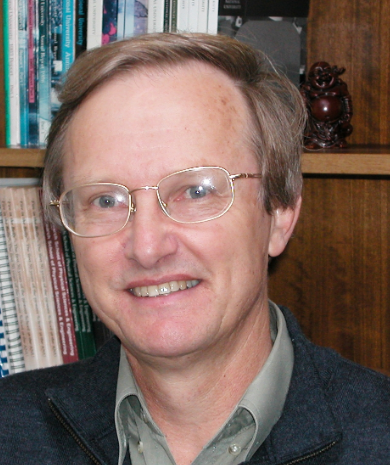 Jim Williams合作论文数College of Science, Australian National University;Acton Semiconductors (Aust) Pty Ltd;Research School of Physical Sciences and Engineering, Australian National University16
 Andrew Dzurak合作论文数School of Electrical Engineering & Telecommunications, The University of New South Wales;Diraq15
 Alastair Stacey合作论文数School of Physics, University Of Melbourne14
 Philipp Reineck合作论文数14
 Arne Laucht合作论文数School of Electrical Engineering & Telecommunication, University of New South Wales Sydney;ARC Centre of Excellence for Quantum Computation and Communication Technology, University of New South Wales Sydney;Ultra-Low Temperature Optics Laboratory, University of New South Wales Sydney14Nikolai Dontschuk合作论文数School of Physics, Faculty of Science, The University of Melbourne13
 Andrew Greentree合作论文数ARC Centre of Excellence for Nanoscale BioPhotonics, RMIT University;School of Science, RMIT University13
 Steven Prawer合作论文数Division of Science, The University of Melbourne13
 Fay Hudson合作论文数School of Electrical Engineering and Telecommunications, The University of New South Wales;Diraq;The Australian National Fabrication Facility12
 Rose Ahlefeldt合作论文数Research School of Physics and Engineering, The Australian National University11
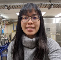 S. Q. Lim合作论文数Res Sch Phys, Australian Natl Univ10
 A. Lyasota合作论文数Sch Phys, Univ New South Wales10
 David Broadway合作论文数Univ Melbourne, Sch Phys, Ctr Quantum Computat & Commun Technol, Melbourne, Vic 3010, Australia10
 Kohei M. Itoh (伊藤公平)合作论文数Department of Applied Physics and Physico-Informatics, Faculty of Science and Technology, Keio University10
 S. Rubanov合作论文数Inst Bio21, University of Melbourne10
 Jodie Bradby合作论文数Physics Education Centre, Research School of Physics, College of Science and Medicine, The Australian National University;Department of Materials Physics, Research School of Physics, College of Science and Medicine, The Australian National University;Australian Institute of Physics10Bin-Bin Xu合作论文数8Simon G. Robson合作论文数8
 Daniel Creedon合作论文数CSIRO8
 Bianca Haberl合作论文数Neutron Scattering Division, Neutron Sciences Directorate, Oak Ridge National Laboratory8Tetienne J-P合作论文数8
 Lohrmann Alexander合作论文数School of Physics, University of Melbourne8
 D. W. M. Lau合作论文数ARC Ctr Excellence Nanoscale BioPhoton, RMIT Univ8
 Jarryd Pla合作论文数UCL, London Ctr Nanotechnol8Hannes Firgau合作论文数7
 Ian Berkman合作论文数7D. Holmes合作论文数7
 John G. Bartholomew合作论文数CALTECH, Kavli Nanosci Inst, Pasadena, CA 91125 USA7Mateusz T Mądzik合作论文数UNSW Sydney, Sch Elect Engn & Telecommun, Ctr Quantum Computat & Commun Technol, Sydney, NSW 2052, Australia7
 Heike Ebendorff-Heidepriem合作论文数School of Physics, Chemistry and Earth Sciences, Faculty of Sciences, Engineering and Technology, The University of Adelaide;Institute for Photonics and Advanced Sensing, The University of Adelaide7
 Igor Aharonovich合作论文数School of Mathematical and Physical Sciences, Faculty of Science, University of Technology Sydney;Writeitupnow7Xie Shouyi合作论文数7A. C. H. Rowe合作论文数6
 Naoya Iwamoto合作论文数6
 Marco Capelli合作论文数Sch Sci, RMIT Univ6




