This paper introduces a compact and time-efficient reduced-order modelling method for conducting thermal–mechanical analyses and studying material nonlinearities in power electronic modules (PEMs). Thermal–mechanical analyses in reduced-order modelling research typically follow a sequential coupling approach, where the thermal model is solved first, allowing the resulting temperature distributions to serve as loads in the mechanical system. In this study, a direct coupling method is employed for the thermomechanical analysis, enabling the simultaneous evaluation of the thermal and structural governing equations to determine thermal and directional deformation distributions, with temperature and deformations as the degrees of freedom (DOFs) of the coupled system. A novel approach, utilising the Krylov subspace-based model order reduction (MOR) process, the Newmark and Newton–Raphson algorithms within the reduced-order modelling framework, have been developed for analysing material nonlinearity in PEMs. The time domain responses, i.e., the transient ROM solutions, align remarkably well with the corresponding FOM solutions. The inelastic strains and plastic work results demonstrate strong consistency for materials having time-independent (plasticity) and time-dependent (creep and viscoplasticity) nonlinearities. Responses of the reduced-order model (ROM) in the frequency (Laplace) domain are analysed in contrast to its full-order model (FOM) to evaluate its characteristics and show suitability within the required expansion points. The MOR process provides a significantly compact ROM order of just 20×20 for reduced-dimensional computation, achieving up to an 83% reduction in computational time compared to its FOM order of approximately 400,000×400,000. The reduced-order modelling approach is implemented using the MATLAB coding environment.
Heterogeneous integration (HI) of electronics components is broadly recognized as a powerful and crucial enabler for the continued growth of computing and communication. From 2010 onwards, the value of HI is increasingly visible in the advanced packaging used in artificial intelligence, high-performance computing, smartphones and communications product implementations. In this Perspective, we argue that HI is crucial to semiconductors and more broadly to the continued evolution of computing and communications. We use leading-edge advanced packaging examples to represent the value, advancements and opportunities for HI. To succeed, it is critical to develop comprehensive HI roadmaps that inform collaborations across the design, manufacturing and reliability spectrum between systems architects, packaging and semiconductor technologists to common goals. Although this article does not provide a full roadmap, we instead detail additional parameters for artificial intelligence, smartphone and other cellular communication devices, and their constituent building blocks including interconnects, power electronics, photonics, thermal management, reliability, modelling and co-design, to foster greater collaboration opportunities among academia, research laboratories and industry. Heterogeneous integration is essential to advances in artificial intelligence, high-performance computing and mobile technologies. This Perspective outlines the emerging technology and challenges necessary to revise the technology roadmap to shape the future evolution of semiconductor systems and computing architectures.
Real-time, high-throughput applications such as AI/ML and connected vehicles require advanced packaging with heterogeneous integration for high performance and thin form factors. Underfills delaminate or crack due to interfacial stresses and stress concentrations, motivating modeling approaches to capture resulting failure modes and effects. While cracks in the underfill (bulk and interfacial) will not immediately affect the operational performance of the package, it will reduce the overall reliability of the electronic package because of the changes in the load distribution. It is necessary to have a simplified modelling scheme to quantify the effect of underfill cracks on the stress distribution in the die, μbumps, and redistribution layers (RDL) of the substrate. A multiscale global-local finite element thermal cycling simulation in the range between -55 and 125 °C is conducted in this paper to assess the effect of the underfill interfacial delamination on the thermomechanical reliability of an advanced heterogeneously integrated multi-chiplet semiconductor package on an ultra-fine pitch organic substrate. A global model with simplified geometry, a coarse mesh, and linear elastic material properties is first developed for the overall package. Local models of the critical region with more detailed geometric features, finer meshes, and nonlinear viscoplastic material properties are seeded with cracks of varying sizes at the underfill interfaces. Stress, strain, and energy distributions are compared in the die, μbump, and RDL, before and after underfill-RDL delamination.
Fan-out wafer-level packaging (FOWLP) addresses the demand for higher interconnect densities by offering reduced form factor, improved signal integrity, and enhanced performance. However, FOWLP faces several manufacturing challenges, such as coefficient of thermal expansion (CTE) mismatch, warpage, die shift, and postmolding protrusion, causing misalignment and bonding issues during redistribution layer (RDL) buildup. In order to address these challenges, we propose a comprehensive defect analysis and testing framework for FOWLP interconnects. We use Ansys Q3D to map defects to equivalent electrical circuit models and perform fault simulations to investigate the impacts of these defects on chiplet functionality. Additionally, we present a built-in self-test (BIST) architecture to detect stuck-at (SA) and bridging faults while accurately diagnosing the fault type and location. We also show how fault signatures can be propagated and decoded across multichiplet interfaces to initiate dynamic repair. To enhance postfabrication yield and reliability, we introduce a priority-based dynamic repair scheme aligned with the universal chiplet interconnect express (UCIe) specification that maximizes repairability without incurring additional hardware overhead in the I/O PHY. This framework offers a practical path toward robust and efficient testability in the next-generation advanced packaging.
Fan-out wafer-level packaging (FOWLP) addresses the demand for higher interconnect densities by offering reduced form factor, improved signal integrity, and enhanced performance. However, FOWLP faces manufacturing challenges such as coefficient of thermal expansion (CTE) mismatch, warpage, die shift, and post-molding protrusion, causing misalignment and bonding issues during redistribution layer (RDL) buildup. Moreover, the organic nature of the package exposes it to severe thermo-mechanical stresses during fabrication and operation. In order to address these challenges, we propose a comprehensive defect analysis and testing framework for FOWLP interconnects. We use Ansys Q3D to map defects to equivalent electrical circuit models and perform fault simulations to investigate the impacts of these defects on chiplet functionality. Additionally, we present a built-in self-test (BIST) architecture to detect stuck-at and bridging faults while accurately diagnosing the fault type and location. Our simulation results demonstrate the efficacy of the proposed BIST solution and provide critical insights for optimizing design decisions in packages, balancing fault detection and diagnosis with the cost of testability insertion.
Heterogeneous integration of chiplets supported by advanced semiconductor packaging technologies is seeing tremendous growth worldwide. These technologies provide advantages compared to homogeneous integration (e.g. system on chip) in terms of improved time to market, improved yield, and the ability mix and match diver IP into a single package with high bandwidth, and low latency. This paper discussed the reliability and associated modelling challenges for these advanced packaging architectures that need to be addressed.
This work presents a new approach for performing a parametric study and examining nonlinear material behaviours of a coupled thermal-mechanical model of a Power Electronics Module (PEM) by integrating the Finite Element Method (ANSYS-FEM) with Parametric Model Order Reduction (pMOR). The considered coupling method solves the thermal and structural models concurrently compared to the widely practised sequential coupling method. Instead of constant parameter values, which are generally regarded for pMOR studies, the temperature-dependent material properties of the wire material have been parametrised in the work using the pMOR method. A generalised 2D model has been regarded here for thermal-mechanical analysis with the pMOR approach, parametrising temperature-dependent coefficient of thermal expansion (CTE) and Young's modulus (E) of the wire material to explore their impact on wire bonds. The matrix interpolation method has been applied here for the pMOR study, and PRIMA, a Krylov subspace-based model order reduction (MOR) technique, has been exercised for local model order reductions. A new efficient process of matrix interpolation, based on the Lagrange interpolation technique, has been developed to implement matrix interpolation in the parametric reduced order model (pROM). The local reduced order models (ROMs) have a degree of freedom (DOF) of just 8, compared to the full-order models' (FOMs) of 50,602. The pROM provides an excellent solution and reduces computational time by 84% for the presented case.
Silk is highly susceptible to fade, often resulting in colour loss to the fabric even when displayed in controlled museum environments. This study applies the engineering-inspired Prognostics and Health Management (PHM) approach to assess the remaining useful life (RUL) of silk fabric in a museum environment, focussing on predicting colour fade as an indicator of degradation. A novel mathematical model is developed to forecast cumulative colour fade of silk upholstery exhibited at the Great Gallery in The Wallace Collection, London. Unlike traditional accelerated aging methods, this model utilises naturally aged samples to estimate the rate of colour change over time. The main contribution of this work lies in the methodology and computational framework for model development using environmental data and conditions of silk in the museum environment. The proposed PHM methodology allows for continuous modifications of the colour fade model to improve accuracy by deploying new data from different silk collections and environments. The article demonstrates a model-based approach for informed decision making in museums regarding display and storage of silk upholstery.
This paper presents a compact and time-efficient reduced-order modelling method for thermal-mechanical analysis and material nonlinearity study of power electronics modules (PEMs). Generally, the thermal-mechanical analyses in research are conducted utilising a sequential coupling method, where the thermal model is solved first, and the temperature distributions are used as a load in the structural (mechanical) system. The direct-coupling method has been employed in the present thermomechanical analysis to evaluate the thermal and structural governing equations together, i.e., to solve for its thermal and directional deformation distributions, which are degrees of freedom (DOFs) of the coupled system. A new approach, utilising the Krylov-subspace- and Arnoldi-based model order reduction (MOR) technique, Newmark method and Newton-Raphson al-gorithm within the reduced-order modelling framework, has been developed and demonstrated here for analysing material nonlinearity of PEMs. The reduced-order model (ROM) solutions agree exceptionally well with the full-order (FOM) solutions, showing excellent consistency in inelastic strains and plastic work results for materials with time-independent and time-dependent nonlinearities. The MOR method offers a remarkably compact model with a ROM order of just 20x20 for reduced-order computation compared to a FOM order of about 400,000x400,000 and up to 83% reduction in computational time.
Ongoing technological advances in photodetector material growth and processing, readout integrated circuits, and robust hybridization (packaging) methods for assembling high-resolution and small-pitch size pixel arrays are the main enabling factors for pushing the frontiers of high-performance Focal Plane Array (FPA) technologies for imaging systems. This paper details the development of analytical and numerical models and demonstrates their use to generate insights into the feasibility of two flip-chip assembly processes for packaging infrared (IR) detector chips. The modeling studies focus on the challenges of forming the indium interconnection arrays in the case of the FPA technologies using Group III-V compound semiconductor materials and ultra-fine pitch pixel array layouts. The accurate alignment of the IR detector chip onto the readout chip in the case of high-density pixel architectures is a critical requirement for the packaging process. To gain a better understanding of this requirement, which has a clear implication for the quality and subsequent reliability performance of the FPA, compression, and reflow bonding process models are developed using suitable modeling approaches and methods and then demonstrated for two distinctive focal plane array design configurations. The novelty of this work is in the developed modeling capabilities utilizing different computational methods, from large deformation and contact analysis finite element to energy-based and harmonic motion mechanics, to characterize and optimize the mechanical and dynamic non-linear behavior of the indium solder joints and their formation during FPA packaging. The feasibility of bonding techniques for different resolution FPAs and under flip-chip misalignment conditions is assessed. The modeling results pointed to a very strict, sub-micrometer flip-chip placement accuracy requirement for the assembly of FPAs with ultra-fine indium bump array resolution.
A damage mechanics-based numerical approach for the prediction of the damage evolution in wirebond structures of the power electronic module (PEM) is presented. A simplistic damage evolution model is developed in an in-house finite element code, with a demonstration focused on the analysis of the wirebond damage evolution by thermally induced stresses in PEM subjected to varying thermal loads. The novelty of the proposed methodology is the damage evolution realized at the level of each discretised mesh element of the finite element model of the PEM structure in the numerical approach and the associated impact of damage on the mechanical material properties of that element. A simplified PEM structure is utilised as a case study to demonstrate the proposed damage evolution modelling. The thermal load of each discretised element of the PEM structure was imported from an external thermal code. From the thermally induced stresses, plastic strain rates were approximated and then, using these metrics a damage evolution metric was derived. The damage distribution plot of the wirebond structure for the applied load in the case study indicates that maximum damage accumulation at the heel structure reaches 2.4% of the total damage after 3 seconds. By extrapolating the trendline of damage evolution in wirebond, the time of the structural failure was also predicted. The maximum von Mises stress was observed on the busbar which reaches 64 MPa. The extreme stresses found at the busbar are attributed to the high value of the coefficient of thermal expansion of the busbar material.
Purpose This study aims to provide an insight into the relationship between design parameters and thermal performance of plate fin heat sinks (PFHSs) incorporating longitudinal vortex generators (VGs) inside a PFHS channel. Design/methodology/approach A computational fluid dynamics model of a delta winglet pair VG mounted inside a PFHS geometry is detailed, and the model is validated by comparison with experimental data. The validated model is used to perform a virtual design of experiments study of the heat sink with bottom plate and vertical plate mounted VGs. Data from this study is used to regress a response surface enabling the influence of each of the assessed design variables on thermal performance and flow resistance to be determined. Findings The results of this study show that the thermal hydraulic performances of a PFHS with bottom plate mounted VG and vertical plate fin mounted VG are, respectively, 1.12 and 1.17 times higher than the baseline PFHS. Further, the performance variation of the heat sink with VG, relative to delta winglet’s arrangement (common flow up and common flow down), trailing edge gap length and Reynolds number were also evaluated and reported. Originality/value For the first time, performance characteristics of delta winglet VGs mounted inside the PFHS are evaluated against different design variables and a polynomial regression model is developed. The developed regression model and computed results can be used to design high performance PFHSs mounted with delta winglet VGs.
The techniques of extended finite element method, level set method and the submodelling approach are implemented in this study to model crack and crack growth in ultrasonically bonded thick aluminium wire for the IGBT power electronics modules under different loading conditions for the purpose of lifetime prediction and reliability assessment during design and manufacturing stages. The crack growth and lifetime prediction were performed under cyclic fatigue passive thermal cycling and active power cycling for the bond wire lift-off failure mechanism while the J-integral for different heel crack lengths are predicted under mechanical loads. The analyses showed that the techniques implemented in this paper are effective for modelling such complex geometries and loading conditions and can easily be integrated in a virtual design platform for power electronics. The accuracy of the technique is evaluated by comparing with trends in the published experimental tests and simulation results as well as the standard finite element method which are all in a good agreement. The wire bond crack growth rate under cyclic loading is strongly influenced by the bond thickness and loading conditions.
Purpose The purpose of the study is to optimise the cross-sectional shape of passively cooled horizontally mounted pin-fin heat sink for higher cooling performance and lower material usage. Design/methodology/approach Multi-objective shape optimisation technique is used to design the heat sink fins. Non-dominated sorting genetic algorithm (NSGA-II) is combined with a geometric module to develop the shape optimiser. High-fidelity computational fluid dynamics (CFD) is used to evaluate the design objectives. Separate optimisations are carried out to design the shape of bottom row fins and middle row fins of a pin-fin heat sink. Finally, a computational validation was conducted by generating a three-dimensional pin-fin heat sink using optimised fin cross sections and comparing its performance against the circular pin-fin heat sink with the same inter-fin spacing value. Findings Heat sink with optimised fin cross sections has 1.6% higher cooling effectiveness than circular pin-fin heat sink of same material volume, and has 10.3% higher cooling effectiveness than the pin-fin heat sink of same characteristics fin dimension. The special geometric features of optimised fins that resulted in superior performance are highlighted. Further, Pareto-optimal fronts for this multi-objective optimisation problem are obtained for different fin design scenarios. Originality/value For the first time, passively cooled heat sink’s cross-sectional shapes are optimised for different spatial arrangements, using NSGA-II-based shape optimiser, which makes use of CFD solver to evaluate the design objectives. The optimised, high-performance shapes will find direct application to cool power electronic equipment.
This paper presents the Tiled Computing Array (TCA), a simple, uniform, 3D-mesh packaging at inter-board level, for massively parallel computers. In particular, the power modelling and practical feasibility of the system is examined. TCA eliminates the need for hierarchical rackmount-structures and introduces short and immediate data channels in multiple physical orientations, allowing a more direct physical mapping of 3D computational topology to real hardware. A dedicated simulation platform has been developed, and an engineered prototype demonstrator has been built. This paper explores the feasibility of the TCA concept for current hardware technologies and systems, evaluates power modeling and validation, and highlights some of the novel design challenges associated with such a system. Evaluations of physical scalability toward large-scale systems are reported, showing that TCA is a promising approach.
This paper presents a multi-scale modelling approach to investigate the underpinning mechanisms of microstructure-sensitive damage of single crystal Sn-3Ag-0.5Cu (wt%, SAC305) solder joints of a Ball Grid Array (BGA) board assembly subject to thermal cycling. The multi-scale scheme couples board-scale modelling at the continuum macro-scale and individual solder modelling at the crystal micro-scale. Systematic studies of tin crystal orientation and its role in fatigue damage have been compared to experimental observations. Crystallographic orientation is examined with respect to damage development, providing evidence-based optimal solder microstructural design for in-service thermomechanical fatigue.
This paper presents the development of a novel modelling approach, based on the use of deep learning (DL), to predict the orthotropic composite properties of copper-patterned conductive layers of printed circuit boards (PCBs). This data is needed to assess the bulk PCB properties with existing methods for laminar composites. Image datasets of copper patterned artwork, required with this approach, are gathered and the composite (homogenised) orthotropic elastic modulus of the respective conductive layouts is evaluated through an automated, macro-script executed, finite element analyses. The modulus values are assigned as labels to each image of a copper layout in the dataset. A regression convolutional neural network is developed and optimised using a training dataset and validated using the test dataset.The results show that the DL model can predict the orthotopic values of the elastic modulus of highly non-structured copper patterns accurately, with the absolute errors of the predicted vs. true (FEA evaluated) property value being less than 3% of the composite propriety range for 99% of the patterns in the validation dataset. The advantages of the proposed machine learning solution over existing techniques are that it can be digitalised and made available to the end-user as an easy-to-use and computationally fast toolset. The modelling approach can enable design engineers effectively explore PCB design alternatives, with awareness of their thermo-mechanical properties and the effect they have on the assembly performance and components' reliability.
The use of semiconductor packages, modules, and printed circuit boards for high-reliability applications, such as the aerospace sector, poses several challenges for original equipment manufacturers (OEMs). Unlike the commercial electronics market, the number of semiconductors used in markets such as aerospace, oil & gas, etc, is tiny, but their reliability requirements are very high. This paper details several ruggedization processes used to address the challenges faced by packages when used in high-reliability applications and demonstrates how modeling and simulation, supported by advanced metrology methods, can help implement commercial-off-the-shelf semiconductor packages.
This article compares the thermomechanical behavior of 3-D inkjet-printed microelectronics devices relative to those fabricated from traditional methods. It discusses the benefits and challenges in the adoption of additive manufacturing methods for microelectronics manufacture relative to conventional approaches. The critical issues related to the design and reliability of additively manufactured parts and systems stem from the change in the manufacturing process and the change in materials utilized. This study uses numerical modeling techniques to gain insight into these issues. This article is an extension of the same topic presented at the 2018 IEEE Electronics Packaging Technology Conference. An introduction providing an overview of the area, covering salient academic research activities and discussing progress toward commercialization is presented. The state-of-the-art modular microelectronics fabrication system developed within the EU NextFactory project is introduced. This system has been used to manufacture several test samples, which were assessed both experimentally and numerically. A full series of JEDEC tests showed that the samples were reliable, successfully passing all tests. The numerical model assessing the mechanical behavior of an inkjet-printed structure during layer-by-layer fabrication is presented. This analysis predicts that the stresses induced by the UV cure process are concentrated toward the extremities of the part and, in particular, in the lower layers which are constrained by the print platform. Subsequently, a model of a multilayer microelectronics structure undergoing JEDEC thermal cycling is presented. The model assesses the differences in mechanical properties between a conventional FR4/copper structure and an inkjet-printed acrylic/silver structure. The model identified that the influence of the sintering process on subsequent material properties, behavior of the inject-printed structure, and reliability of the inject-printed structure is significant. Key findings are that while stresses in the conventional and inkjet boards are relatively similar, the inkjet-printed board exhibits significantly greater deformation than the standard board. Furthermore, the mechanical stresses in the inkjet fabricated board are strongly dependent on the elastic modulus of the sintered silver material, which, in turn, is dependent on the sintering process.
 stoyan stoyanov合作论文数122
 Lu Hua (华潞)合作论文数Fuwai Hospital, CAMS & PUMC%_%National Center for Cardiovascular Diseases72
 Tim Tilford合作论文数1;School of Computing and Mathematical Sciences;University Of Greenwich;School of Computing and Mathematical Sciences, University Of Greenwich64
 Chunyan Yin (尹春燕)合作论文数School of Integrated Circuits, Southeast University60
 Marc Desmulliez合作论文数Research Institute of Signals, Sensors and Systems, School of Engineering and Physical Sciences, Heriot-Watt University;MIcrosystems Engineering Centre, Heriot Watt University58
 Mark Cross合作论文数College of Engineering, Swansea University45
 Koulis A. Pericleous合作论文数School of Computing and Mathematical Sciences, Faculty of Liberal Arts and Sciences, University of Greenwich38
 Pushparajah Rajaguru合作论文数37
 Mayur Patel合作论文数School of Computing and Mathematical Sciences, Faculty of Engineering and Science, University of Greenwich37
 Yan Cheong Chan (陳忍昌)合作论文数Department of Electronic Engineering, City University of Hong Kong35
 M.J. Rizvi合作论文数School of Computing and Mathematical Sciences, University of Greenwich22
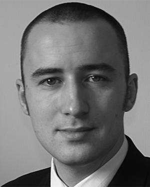 K. I. Sinclair合作论文数17
 David Flynn合作论文数Heriot-Watt University16Xiangdong Xue合作论文数16
 M. O. Alam合作论文数Department of Electronic Engineering;City University of Hong Kong;Department of Electronic Engineering, City University of Hong Kong16Mark Johnson合作论文数14P Chow合作论文数12Georgios Tourloukis合作论文数12
 Robert W. Kay合作论文数12stephen ridout合作论文数12
 George Goussetis合作论文数School of Informatics12
 Gareth Taylor合作论文数Department of Electronic and Computer Engineering, Brunel University11
 Mahera Musallam合作论文数11d gwyer合作论文数10Nadia Strusevich合作论文数10
 Sumanth Kumar Pavuluri合作论文数Microsyst. Eng. Centre (MISEC),, Heriot-Watt Univ.;c;Microsyst. Eng. Centre (MISEC),, Heriot-Watt Univ.10
 Catherine Tonry合作论文数School of Computing and Mathematical Sciences, Faculty of Engineering and Science, University of Greenwich10
 Paul Stewart合作论文数10A. K. Slone合作论文数10V Fomin合作论文数9Y. Benveniste合作论文数9
 Christopher Hunt合作论文数9Ying Kit Tang合作论文数9Manabu Iguchi (井口学)合作论文数Osaka Metropolitan University9
 Shuchen Hsieh (謝淑貞)合作论文数Department of Chemistry, National Sun Yat-Sen University;Center for Green-Energy Key Materials Research;School of Pharmacy, Kaohsiung Medical University9
 Adrian Bejan合作论文数Thomas Lord Department of Mechanical Engineering & Materials Science, Pratt School of Engineering, Duke University9
 Kevin Mcmanus合作论文数9
 Tayfun E. Tezduyar合作论文数Faculty of Science and Engineering, Waseda University9
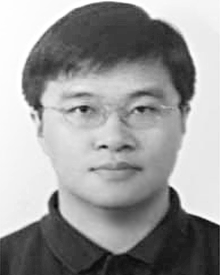 Hsien-Chie Cheng合作论文数9
 Matej Daniel合作论文数Department of Orthopaedic Surgery, Medical Center9Wen Jong Wu合作论文数8g moran合作论文数8P Misselbrook合作论文数8
 manisekaran santhanakrishnan合作论文数Department of Mathematical Sciences, University of Greenwich8
 Mominul Ahsan合作论文数Corresponding author.8Strusevich, N.合作论文数8
 Alan J. Sangster合作论文数8a k parrott合作论文数7peter mason合作论文数7




