Microfluidics is a rapidly expanding field and microfluidic devices have been used in a variety of biomedical applications such as cell sorting, disease diagnostics and various lab-on-a-chip systems. There is great demand for manufacturing techniques capable of fabricating ever more intricate microstructures for increasingly complex applications whilst remaining cost-effective for use in biomedical research. Conventional manufacturing techniques can be used to fabricate many complex microchannel architectures but are often expensive, low throughput, have poor microfeature resolution or are unsuitable to be used at scale. To address this issue, we describe a manufacturing technique that employs stereolithography 3D printing to produce a base substrate which can be sealed with a laser patterned adhesive layer cover and stacked in a compact configuration. The technique provides for the design and manufacturing of a device that can bemassively parallelized at relatively low cost and with a small laboratory footprint. This paper aims to fully explain the design and manufacturing process undertaken to allow the use of this technique in future research.
Transition-edge sensors (TESs) have the potential to perform electron spectroscopic measurements with far greater measurement rates and efficiencies than can be achieved using existing electron spectrometers. Existing spectrometers filter electrons by energy before detecting a narrow energy band at a time, discarding the vast majority of electrons available for measurement. In contrast, TESs have intrinsic energy sensitivity and so do not require prior filtering to perform energy-resolved measurements. Despite this fundamental advantage, TES electron spectroscopy has not, to our knowledge, previously been reported in the literature. We present the results of a set of proof-of-principle experiments demonstrating TES electron spectroscopy experiments using Mo/Au TESs repurposed for electron calorimetry. Using these detectors, we successfully measured the electron spectrum generated by an electron beam striking a graphite target with energies between 750 and 2000 eV, at a noise-limited energy resolution of 4 eV. Based on the findings of these experiments, we suggest improvements that could be made to TES design to enhance their electron detection capabilities through the use of a dedicated electron absorber in the device with integrated electron optics.
We consider and compare candidate superconducting detector technologies that might be applied to the readout of cavity-axion haloscopes and similar fundamental physics experiments. We conclude that a transition edge sensor (TES) configured with ballistic-phonon thermal isolation operated with a superconducting transition temperature of order 30 mK would provide quantum-limited detection performance at frequencies above 5 GHz. This would permit the realisation of integrated homodyne detectors based on TESs that we believe would make a unique contribution to a variety of fundamental physics experiments, particularly those based on reading out microwave cavities in the quantum ground state.
Understanding the magnetic field sensitivity of transition edge sensors (TESs) is vital in optimising the configuration of any magnetic shielding as well as the design of the TESs themselves. An experimental system has been developed to enable the investigation of the applied magnetic field direction on TES behaviour, and the first results from this system are presented. In addition, measurements of the effect of applied magnetic field magnitude on both supercurrent and bias current are presented. The extent to which the current theoretical framework can explain the results is assessed and finally, the impact of this work on the design of TESs and the design of magnetic shielding is discussed.
Neutrino oscillation experiments show that neutrinos have mass; however, the absolute mass scale is exceedingly difficult to measure and is currently unknown. A promising approach is to measure the energies of the electrons released during the radioactive decay of tritium. The energies of interest are within a few eV of the 18.6 keV end point, and so are mildly relativistic. By capturing the electrons in a static magnetic field and measuring the frequency of the cyclotron radiation emitted the initial energy can be determined, but end-point events are infrequent, the observing times short, and the signal to noise ratios low. To achieve a resolution of < 10 meV, single-electron emission spectra need to be recorded over large fields of view with highly sensitive receivers. The principles of Cylotron Radiation Emission Spectroscopy (CRES) have already been demonstrated by Project 8, and now there is considerable interest in increasing the FoV to > 0.1 m^3. We consider a range of issues relating to the design and optimisation of inward-looking quantum-noise-limited microwave receivers for single-electron CRES, and present a single framework for understanding signal, noise and system-level behaviour. Whilst there is a great deal of literature relating to the design of outward-looking phased arrays for applications such as radar and telecommunications, there is very little coverage of the new issues that come into play when designing ultra-sensitive inward-looking phased arrays for volumetric spectroscopy and imaging.
In this work, we study the effects of a transverse magnetic field in a Kondo lattice model with twoforbitals interacting with the conduction electrons. Thefelectrons that are present on the same site interact through Hund's coupling, while on neighboring sites they interact through intersite exchange. We consider here that part offelectrons are localized (orbital 1) while another part (orbital 2) are delocalized, as it is frequent in uranium systems. Then, only electrons in the localized orbital 1 interact through exchange interaction with the neighboring ones, while electrons in orbital 2 are coupled with conduction electrons through a Kondo interaction. We obtain a solution where ferromagnetism and Kondo effect coexist for small values of an applied transverse magnetic field forT→0. Increasing the transverse field, two situations can be obtained when Kondo coupling vanishes: first, a metamagnetic transition occurs just before or at the same time of the fully polarized state, and second, a metamagnetic transition occurs when the spins are already pointing out along the magnetic field.
The appearance of an incommensurate charge density wave vector $\textbf{Q} = (Q_x,Q_y)$ on multiband intermetallic systems presenting commensurate charge density wave (CDW) and superconductivity (SC) orders is investigated. We consider a two-band model in a square lattice, where the bands have distinct effective masses. The incommensurate CDW (inCDW) and CDW phases arise from an interband Coulomb repulsive interaction, while the SC emerges due to a local intraband attractive interaction. For simplicity, all the interactions, the order parameters and hybridization between bands are considered $\textbf{k}$-independent. The multiband systems that we are interested are intermetallic systems with a $d$-band coexisting with a large $c$-band, for which a mean-field approach has proved suitable. We obtain the eigenvalues and eigenvectors of the Hamiltonian numerically and minimize the free energy density with respect to the diverse parameters of the model by means of the Hellmann-Feynman theorem. We investigate the system in real as well as momentum space and we find an inCDW phase with wave vector $\textbf{Q} = (\pi, Q_y) = (Q_x, \pi)$. Our numerical results show that the arising of an inCDW state depends on parameters, such as the magnitude of the inCDW and CDW interactions, band filling, hybridization and the relative depth of the bands. In general, inCDW tends to emerge at low temperatures, away from half-filling. We also show that, whether the CDW ordering is commensurate or incommensurate, large values of the relative depth between bands may suppress it. We discuss how each parameter of the model affects the emergence of an inCDW phase.
Superconducting resonators and parametric amplifiers are important components in scientific systems such as kinetic inductance detector arrays, frequency-domain multiplexers for other superconducting bolometers, spin-ensemble based memories, and circuit quantum electrodynamics demonstrators. In this paper, we report microwave measurements of superconducting Ti, Nb, and NbN resonators and their use as parametric amplifiers. These half-wave resonators were fabricated under near identical sputtering and lithographic conditions to ensure a like-for-like comparison of material properties. We report a wide range of properties and behaviours in terms of transition temperatures, resistivities, rate-limiting nonlinear response times, nonlinear dissipation, signs of the nonlinear inductances and their dependences on temperature and resonance harmonic. We have successfully operated Nb and NbN resonators as high gain parametric amplifiers, achieving greater than 20 dB of power amplification. We have shown that for a half-wave resonator, amplification can be realised not only in the fundamental resonance but also in the higher harmonic resonances. Further, for materials with high transition temperatures, e.g. Nb and NbN, amplification can be achieved at ∼4 K, i.e. a temperature maintained by a pulse tube cooler. Finally, in materials systems that have very fast response times, e.g. NbN, we have found that a cross-harmonic type of amplification can be achieved by placing pump tone in a different resonant mode as the signal and the idler. This wide range of observations will have important implications on the design and application of superconducting parametric amplifiers.
Transition-edge sensors (TESs) have found a wide range of applications in both space- and land-based astronomical photon measurement and are being used in the search for dark matter and neutrino mass measurements. A fundamental aspect of TES physics that has not been investigated is the sensitivity of TESs to strong DC electric fields (10 kV/m and above). Understanding the resilience of TESs to DC electric fields is essential when considering their use as charged particle spectrometers, a field in which TESs could have an enormous impact. Techniques such as x-ray photoelectron spectroscopy produce a high number of low-energy electrons that are not of interest and can be screened from the detector using electrostatic deflection. The use of strong electric fields could also provide a mass-efficient route to prevent secondary electron measurements arising from cosmic radiation in space-based TES applications. Integrating electron optics into the TES membrane provides an elegant and compact means to control the interaction between charged particles and the sensor, whether by screening unwanted particles or enhancing the particle absorption efficiency but implementing such techniques requires understanding the sensitivity of the TES to the resulting electric fields. In this work, we applied a uniform DC electric field across a Mo/Au TES using a parallel pair of flat electrodes positioned above and below the TES. The electric field in the vicinity of the TES was enhanced by the presence of silicon backing plate directly beneath the TES. Using this arrangement, we were able to apply of electric fields up to 90 kV/m across the TES. We observed no electric field sensitivity at any field strength demonstrating the capability to use TESs in environments of strong electric fields.
The underlying nonlinear mechanisms behind the operation of travelling-wave parametric amplifiers (TWPAs) are important in determining their performance in terms of added noise, maximum gain, and bandwidth. We describe a method of characterising the underlying nonlinearity of a superconducting material in terms of its dissipative-reactive ratio and the response time of the underlying microscopic processes. We describe and calculate the different behaviour arising from the equilibrium supercurrent nonlinearity , which has low dissipation and fast response time, and the non-equilibrium heating nonlinearity , which has high dissipation and slow response time. We have fabricated TWPAs based on Al and Ti, and characterised their nonlinearities using our analysis. For both Al and Ti, the measured dissipative-reactive ratios and response times are quantitatively similar to predictions for the non-equilibrium heating nonlinearity. We were able to obtain more than 20 d B of peak power gain, although only over a narrow bandwidth of a few kilohertz. Our method of characterising the underlying nonlinearities could also be useful in the understanding and design of other superconducting nonlinear devices such as parametric up-converters, kinetic inductance Fourier transform spectrometers, and resonator parametric amplifiers.
Far-infrared detectors for future cooled space telescopes require ultra-sensitive detectors with optical noise equivalent powers of order 0.2 aW/√Hz. This performance has already been demonstrated in arrays of transition edge sensors. A critical step is demonstrating a method of fabrication and assembly that maintains the performance but that is extendable to create large-scale arrays suitable, for example, for application in dispersive spectrometers where it may be advantageous to fabricate the array from smaller sub-arrays. Critical here are the methods of assembly and metrology that maintain the required tolerances on the spatial alignment of the components in order to maintain overall performance. These are discussed and demonstrated.
As in conventional computing, memories for quantum information benefit from high storage density and, crucially, random access, or the ability to read from or write to an arbitrarily chosen register. However, achieving such random access with quantum memories in a dense, hardware-efficient manner remains a challenge. Here we introduce a protocol using chirped pulses to encode qubits within an ensemble of quantum two-level systems, offering both random access and naturally supporting dynamical decoupling to enhance the memory lifetime. We demonstrate the protocol in the microwave regime using donor spins in silicon coupled to a superconducting cavity, storing up to four weak, coherent microwave pulses in distinct memory modes and retrieving them on demand up to 2 ms later. This approach offers the potential for microwave random access quantum memories with lifetimes exceeding seconds, while the chirped pulse phase encoding could also be applied in the optical regime to enhance quantum repeaters and networks.
We present a formalism for modelling parametric amplification by resonators subject to rate-limited nonlinearity of mixed reactive/dissipative character, with particular relevance to superconducting devices. The non-linearity is assumed to be characterised by a single state parameter, which responds to changes in the energy stored in the resonator with finite response time. We show how the operating point and small signal amplification behaviour of the pumped resonator can be calculated, characterised and optimised in terms of a set of three dimensionless parameters. The formalism is then illustrated with a simple, first-order, model nonlinearity and the implications for amplification via quasiparticle generation in a superconductor discussed. Throughout we describe how the parameters needed to characterise the device can be determined experimentally from steady-state measurements. A key result of this paper is that rate-limiting of a nonlinear mechanism does not preclude amplification, although it does limit the bandwidth over which it may be achieved.
Transition-edge sensors (TESs) are capable of highly accurate single particle energy measurement. TESs have been used for a wide range of photon detection applications, particularly in astronomy, but very little consideration has been given to their capabilities as electron calorimeters. Existing electron spectrometers require electron filtering optics to achieve energy discrimination, but this step discards the vast majority of electrons entering the instrument. TESs require no such energy filtering, meaning they could provide orders of magnitude improvement in measurement rate. To investigate the capabilities of TESs in electron spectroscopy, a simulation pipeline has been devised. The pipeline allows the results of a simulated experiment to be compared with the actual spectrum of the incident beam, thereby allowing measurement accuracy and efficiency to be studied. Using Fisher information, the energy resolution of the simulated detectors was also calculated, allowing the intrinsic limitations of the detector to be separated from the specific data analysis method used. The simulation platform has been used to compare the performance of TESs with existing X-ray photoelectron spectroscopy (XPS) analysers. TESs cannot match the energy resolution of XPS analysers for high-precision measurements but have comparable or better resolutions for high count rate applications. The measurement rate of a typical XPS analyser can be matched by an array of 10 TESs with 120 microsecond response times and there is significant scope for improvement, without compromising energy resolution, by increasing array size.
James O’Sullivan, ∗ Oscar W. Kennedy, ∗ Kamanasish Debnath, Joseph Alexander, Christoph W. Zollitsch, Mantas Šimėnas, Akel Hashim, 4 Christopher N. Thomas, Stafford Withington, Irfan Siddiqi, 4 Klaus Mølmer, and John J. L. Morton 6 London Centre for Nanotechnology, UCL, 17-19 Gordon Street, London, WC1H 0AH, UK Department of Physics and Astronomy, Aarhus University, DK-8000 Aarhus C, Denmark Quantum Nanoelectronics Laboratory, Department of Physics, UC Berkeley, California 94720, USA Lawrence Berkeley National Laboratory, Berkeley, CA 94720, USA Cavendish Laboratory, University of Cambridge, JJ Thomson Ave, Cambridge CB3 0HE, UK Department of Electrical and Electronic Engineering, UCL, Malet Place, London, WC1E 7JE, UK
Nei Lopes, ∗ Daniel Reyes, † Mucio A. Continentino, and Christopher Thomas ‡ Departamento de F́ısica Teórica, Universidade do Estado do Rio de Janeiro, Rua São Francisco Xavier 524, Maracanã, 20550-013, Rio de Janeiro, RJ, Brazil Instituto Militar de Engenharia Praça General Tibúrcio, 80, 22290-270, Praia Vermelha, Rio de Janeiro, Brazil Centro Brasileiro de Pesquisas F́ısicas, Rua Dr. Xavier Sigaud 150, Urca, 22290-180, Rio de Janeiro , Brazil Departamento de F́ısica, Universidade Federal Rural do Rio de Janeiro, 23897-000, Seropédica, Rio de Janeiro, Brazil (Dated: March 23, 2021)
We investigated the use of dielectric layers produced by atomic layer deposition (ALD) as an approach to strain mitigation in composite silicon/superconductor devices operating at cryogenic temperatures. We show that the addition of an ALD layer acts to reduce the strain of spins closest to silicon/superconductor interface where strain is highest. We show that appropriately biasing our devices at the hyperfine clock transition of bismuth donors in silicon, we can remove strain broadening and that the addition of ALD layers left T2 (or temporal inhomogeneities) unchanged in these natural silicon devices.
Superconducting thin films are central to the operation of many kinds of quantum sensors and quantum computing devices: kinetic inductance detectors (KIDs), travelling-wave parametric amplifiers (TWPAs), qubits, and spin-based quantum memory elements. In all cases, the nonlinearity resulting from the supercurrent is a critical aspect of behaviour, either because it is central to the operation of the device (TWPA), or because it results in nonideal second-order effects (KID). Here, we present an analysis of supercurrent-carrying superconducting thin films that is based on the generalized Usadel equations. Our analysis framework is suitable for both homogeneous and multi-layer thin films, and can be used to calculate the resulting density of states, superconducting transition temperature, superconducting critical current, complex conductivities, complex surface impedances, transmission line propagation constants, and nonlinear kinetic inductances in the presence of supercurrent. Our analysis gives the scale of kinetic inductance nonlinearity ( I_* ) for a given material combination and geometry, and is important in optimizing the design of detectors and amplifiers in terms of materials, geometries, and dimensions. To investigate the validity of our analysis across a wide range of supercurrent, we have measured the transition temperatures of superconducting thin films as a function of DC supercurrent. These measurements show good agreement with our theoretical predictions in the experimentally relevant range of current values.
We discuss how reactive and dissipative non-linearities affect the intrinsic response of superconducting thin-film resonators. We explain how most, if not all, of the complex phenomena commonly seen can be described by a model in which the underlying resonance is a single-pole Lorentzian, but whose centre frequency and quality factor change as external parameters, such as readout power and frequency, are varied. What is seen during a vector-network-analyser measurement is series of samples taken from an ideal Lorentzian that is shifting and spreading as the readout frequency is changed. According to this model, it is perfectly proper to refer to, and measure, the resonant frequency and quality factor of the underlying resonance, even though the swept-frequency curves appear highly distorted and hysteretic. In those cases where the resonance curve is highly distorted, the specific shape of the trajectory in the Argand plane gives valuable insights into the second-order physical processes present. We discuss the formulation and consequences of this approach in the case of non-linear kinetic inductance, two-level-system loss, quasiparticle generation, and a generic model based on a power-law form. The generic model captures the key features of specific dissipative non-linearities, but additionally leads to insights into how general dissipative processes create characteristic forms in the Argand plane. We provide detailed formulations in each case, and indicate how they lead to the wide variety of phenomena commonly seen in experimental data. We also explain how the properties of the underlying resonance can be extracted from this data. Overall, our paper provides a self-contained compendium of behaviour that will help practitioners interpret and determine important parameters from distorted swept-frequency measurements.
The ability to measure both optical efficiency and dynamic response to changes in optical signal is crucial to the development of Transition Edge Sensors (TESs) for far-infrared astronomical instruments. We have devised and implemented a cryogenic test facility for ultra-low-noise far-infrared TESs, designed for the SAFARI grating spectrometer on the cooled-aperture space telescope SPICA. Whilst our experimental arrangement is suitable for the whole of the SAFARI wavelength range, 34-230 μm, we focus here on representative optical measurements at 60-110 μm. Detectors are illuminated with a few-mode beam having modal characteristics identical to those of an ideal imaging telescope. In addition, a fast thermal infrared source allows direct measurement of the TES response to tiny changes in incident optical power. We describe the measured functional forms of TES transient responses both to fast optical pulses and to modulation of the power dissipated in the bilayer, in the presence of background optical loading through to TES saturation.
 Stafford Withington合作论文数Department of Physics, University of Cambridge53
 David J. Goldie合作论文数26
 Songyuan Zhao合作论文数Cavendish Lab, JJ Thomson Ave, Cambridge CB3 OHE, England9Claudine Lacroix合作论文数Institut Néel, Université Grenoble Alpes8
 Jose Roberto Iglesias合作论文数Inst Fis, Univ Fed Rio Grande do Sul6
 Daniel Reyes Lopez合作论文数6
 Mucio A. Continentino合作论文数Department of Theoretical Physics, Centro Brasileiro de Pesquisas Fisicas6
 Christophe Craeye合作论文数Institute of Information and Communication Technologies, Electronics and Applied Mathematics, Universite Catholique de Louvain;University of Massachusetts;The Netherlands Institute for Research;University of Cambridge6Emily A. Williams合作论文数5R. Sudiwala合作论文数5Bernard Coqblin合作论文数5Acirete S. Da Rosa Simões合作论文数5James O’Sullivan合作论文数4
 Oscar Kennedy合作论文数Dept Phys & Astron, UCL4Zollitsch Christoph W合作论文数4
 Eloy de Lera Acedo合作论文数4
 John Morton合作论文数London Centre for Nanotechnology, University College London4
 Nei Lopes合作论文数3A. Orlando合作论文数3
 Denis Tihon合作论文数ICTEAM Inst., Univ. Catholique de Louvain;c;ICTEAM Inst., Univ. Catholique de Louvain3
 Paul Grimes合作论文数Division of Radio and Geoastronomy, Center for Astrophysics | Harvard & Smithsonian;Smithsonian Astrophysical Observatory, Center for Astrophysics | Harvard & Smithsonian3
 Peter Ade合作论文数School of Physics and Astronomy, Cardiff University3
 Lingzhen Zeng合作论文数3
 Sebastien Burdin合作论文数3
 Joseph Alexander合作论文数2
 Akel Hashim合作论文数Quantum Nanoelect Lab, Univ Calif Berkeley2
 Kamanasish Debnath合作论文数Chalmers University of Technology2
 c pepin合作论文数CNRS, Univ Paris Saclay2
 P. C. Hargrave合作论文数Dept Phys & Astron, Cardiff Univ2
 Irfan Siddiqi合作论文数Quantum Nanoelectronics Laboratory, Department of Physics, University of California, Berkeley2
 Mantas Simenas合作论文数Faculty of Physics, Vilnius University2Glowacka, Dorota M.合作论文数2
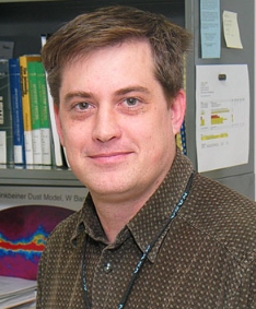 Edward J Wollack合作论文数Goddard Space Flight Center, National Aeronautics and Space Administration2
 Klaus Mølmer合作论文数Niels Bohr Institutet, Københavns Universitet2
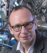 Alexander Shard合作论文数National Physical Laboratory2
 Raymond Blundell合作论文数Department of Astronomy, Harvard University2
 David T. Chuss合作论文数Department of Physics, College of Liberal Arts and Sciences, Villanova University2
 Scott Paine合作论文数2
 Natalia B. Perkins合作论文数Sch Phys & Astron, Univ Minnesota2
 Alvaro Ferraz合作论文数2Rashmi Sudiwala合作论文数2E. Tong合作论文数1S. N. Paine合作论文数1M. Inoue合作论文数1P. Martin-Cocher合作论文数1D. Kubo合作论文数1Ranjani Srinivasan合作论文数1




