The single-event transients (SETs) have become a main contributor to soft errors in deep sub-micrometer integrated circuits applied in space. The sensitivity of 65-nm very large scale integrated circuits (VLSI) to SET, especially to clock SET, is studied by heavy ion experiments and analyzed. Built-in scan chains in the VLSI are utilized for experimental tests and proven to be very useful for SET evaluation. The specially designed test chip is developed and tested to find the relation between errors’ distribution and clock tree structures. Error count per event (EPE) is proposed as a metric of SET, and EPE distribution is found to be able to reflect error sources in the circuit topology. The related mechanisms are analyzed and implications for error positioning and design enhancement are given.
空间应用的集成电路受到辐射效应的影响,会出现瞬态干扰、数据翻转、性能退化、功能失效甚至彻底毁坏等问题.随着器件特征尺寸进入到100nm以下(以下简称纳米级),这些问题的多样性和复杂性进一步增加,单粒子效应成为集成电路在空间可靠性应用的主要问题,给集成电路的辐射效应评估和抗辐射加固带来了诸多挑战.本文以纳米级CMOS集成电路为研究对象,结合近年来国内外的主要技术进展,介绍研究团队在65 nm集成电路单粒子效应和加固技术方面的研究成果,包括首次提出的单粒子时域测试和分析方法、单粒子多节点翻转加固方法和单粒子瞬态加固方法等.
>As technology extends to nanometer scales,the critical charge to induce a single event decreases along with the technology node,and the threshold linear energy transfer(LET)for a soft error also decreases[1].Meanwhile,as the operating frequency of the integrated circuit(IC)increases,the possibility for single event transients(SETs)to be captured increases.Moreover,SETs have
Two 65 nm bulk CMOS test chips, each containing several different types of flip-flop chains, are designed and tested. Heavy ion results are given and analyzed across ion LET and in proposed time domain. The single event upset (SEU) and single event transient (SET) performance of various DFFs are compared and discussed, concluding several practical implications for radiation hardening by design (RHBD). The effectiveness of redundant delay filter (RDF) on mitigating SETs is proven by experiment for the first time.
As high voltage BiCMOS process has been more frequently selected in driver IC design,problems become increasingly outstanding. The requirement of process flexibility and convenience during the design course becomes a new subject. Comparing with normal CMOS device, high voltage transistor is different with special consideration on both process and layout node. Flexibility and adjustability of PDK are key aspects for a successful design. And meanwhile, more devices with better performance can provide competitive options for design house which need innovation on process. In addition, the cooperation between FAB and design house can help to break through the bottle-neck of high voltage process application in driver IC design.
 Liang Wang合作论文数Beijing Microelectronics Technology Institute, Beijing, China4
 Jiaqi Liu合作论文数3Yongshu Sun合作论文数2
 Hongchao Zheng合作论文数Beijing Microelect Technol Inst, Beijing 100076, Peoples R China2
 Tongde Li合作论文数Beijing Microelectronics Technology Institute, Beijing, China2Dongqiang Li合作论文数2
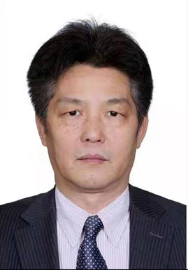 Yuanfu Zhao (赵元富)合作论文数School of Electronics and Information Engineering, Hangzhou Dianzi University2
 Lei Shu (舒磊)合作论文数College of Artificial Intelligence, Nanjing Agricultural University;NAU-Lincoln Joint Research Center of Intelligent Engineering;Beyond Intelligent Phytoprotection Research Institute, Nanjing Agricultural University;School of Engineering, College of Health and Science, University of Lincoln2Suge Yue合作论文数2Zhao Xinyuan合作论文数1
 Hanning Wang (王汉宁)合作论文数School of Integrated Circuits, Tsinghua University1Maoxin Chen合作论文数1
 Yuan Li合作论文数1Long Fan (范隆)合作论文数1Weiping Chen (陈伟平)合作论文数School of Astronautics, Harbin Institute of Technology1
 Lin Liu合作论文数1




