We proposed a novel three-stage CTLE circuit for 12.5Gbps SerDes based on 28nm CMOS process. A cross-coupled negative capacitance structure was adopted to feature more zero poles, the increasing of gain and an adjustable equalization amplitude in single-stage CTLE. As well, a three-stage structure was adopted to feature the gain boost and a favorable eye diagram. At the transmission rate of 12.5Gbps, the proposed circuit demonstrated a single-stage compensation capability of 24.23dB, an output eye-height of 305.38mV, a horizontal jitter control of 0.19UI, and an area of 0.10mm 2 .
Using single event effect sensitivity evaluation test method and test system as well as pulsed laser simulation sources, the SEE sensitivity of High-Speed Serial Interface was experimentally researched. The test results show that the JESD204B high-speed serial transmitter has strong resistance to single-event upset(SEU). The single-event upset sensitive area map of the JESD204B high-speed serial transmitter was obtained through experiments. The single-event upset sensitive unit of the device was located, which provided guidance for the design of high-speed serial interface chips strengthened by radiation resistance.
Abstract This work proposed and discussed a serial JESD204B data receiver and conducted a single event effect test on it. The test is used to analyzed the Single Event Upset (SEU), single Event Latch-up (SEL) and Single Event Functional Interrupt (SEFI). The purpose of the test is to determine if single event effect caused the chip to crash or increase the on-track error rate. The results show that the circuit has a strong ability to resist Single event effect.
A Testing system for transient irradiation experiment is designed to explore the transient ionizing radiation effects in an 8bit three state output bidirectional buffer. Signal responses of this circuit irradiated with high dose rate gamma rays are obtained. In particular, changes of output and supply voltage for the circuit are focused. The experiment results show that the recovery situation of signal depends on the disturbance-rejecting capability of supply voltage.
>As technology extends to nanometer scales,the critical charge to induce a single event decreases along with the technology node,and the threshold linear energy transfer(LET)for a soft error also decreases[1].Meanwhile,as the operating frequency of the integrated circuit(IC)increases,the possibility for single event transients(SETs)to be captured increases.Moreover,SETs have
In this paper, the SEE (single event effects) sensitive mapping of different parts of device is explored in a 32-bit microprocessor with a five-stage instruction pipeline by the laser test. The comparison of the sensitive mapping and the layout of device indicates that they fit well with each other. The method in this paper is a meaningful way to validate the reinforcement effect and to provide guidance for improving reinforcement design by corresponding with the physical layout. The pulsed laser that can locate the sensitive sites is an extremely powerful and useful technique for SEE testing, and will provide invaluable information for characterizing the SEE in integrated circuits.
Single-event effects of nano scale integrated circuits are investigated. Evaluation methods for single-event transients, single-event upsets, and single-event functional interrupts in nano circuits are summarized and classified in detail. The difficulties in SEE testing are discussed as well as the development direction of test technology, with emphasis placed on the experimental evaluation of a nano circuit under heavy ion, proton, and laser irradiation. The conclusions in this paper are based on many years of testing at accelerator facilities and our present understanding of the mechanisms for SEEs, which have been well verified experimentally.
In order to provide guidance for parameter settings in different error rate predicting models and for anti‐irradiation hardened design ,a 32‐bit microprocessor is selected as our target circuit ,and the sensitive depth of circuit is investigated .Utilizing the regional radiation of laser pulses and the adjustability of laser focus panel ,we obtain the sensitive depth of cache areas ,regfile areas and the combinational logic areas which are fabricated in 180 nm CMOS technology .Results show that the sensitive depth of the different sensitive areas in one device is almost the same whose value is about 1μm .Sensitive parameters of the device can be obtained by this approach accurately , conveniently and fast which provide a strong reference to the device for better estimation of the error rate .
The sensitivity of complex integrated circuits to single-event effects is investigated. Sensitivity depends not only on the cross section of physical modules but also on the behavior of data patterns running on the system. A method dividing the main functional modules is proposed. The intrinsic cross section and the duty cycles of different sensitive modules are obtained during the execution of data patterns. A method for extracting the duty cycle is presented and a set of test patterns with different duty cycles are implemented experimentally. By combining the intrinsic cross section and the duty cycle of different sensitive modules, a universal method to predict SEE sensitivities of different test patterns is proposed, which is verified by experiments based on the target circuit of a microprocessor. Experimental results show that the deviation between prediction and experiment is less than 20%.
The single event effects of the sensitivity of a circuit are investigated on a 32-bit microprocessor with a five-stage instruction pipeline by pulsed laser test. The investigation on sensitive mapping of the memory cell is illustrated and then the comparison between the sensitive mapping and the layout of the circuit is made. A comparison result indicates that the area of the sensitive node in sensitive mapping is just the location of the drain in the layout. Therefore, SEE sensitivity in sensitive mapping fits well with that in the physical layout of functional units, which can directly and objectively indicate the size and distribution of sensitive areas. The investigation of sensitive mapping is a meaningful way to verify the hardened effect and provide a reference for improving hardened design by combining with the physical layout.
An experimental system is developed for the transient radiation effects testing of an anti- radiation hardened processor. Based on this system, the transient radiation effects in a microprocessor based on SPARC-V8 architecture was investigated. The dose-rate-soft-error index parameters of the processor were determined according to the test results, as were the influences on the function and timing parameters of the processor. The power supply balance is affected, which caused the system to reset and be the main source of soft errors. The results showed the circuit recovery time is primarily determined by the internal PLL, while the core power and the output-low-IO ports are more sensitive to the transient dose rate effect. The power-integrity-hardened design is proposed to mitigate the transient radiation effect.
This paper presents a NIOS II-based Single Event Effects detection system of asynchronous SRAM,which is used to evaluate the single-event-effect capabilities of anti-radiation hardened SRAM circuit.The detection system can be used for dynamic and static testing of asynchronous SRAM in four operating mode.The experimental data of five kinds' icons are obtained under the heavy ion accelerator by using the detection system with one kind asynchronous SRAM.Single-event-upset threshold、saturated-cross-section and in-orbit-error-rate are taken by statistical analysis of the results,and the results are compared with the same circuit abroad.Based on these experiment results,the assessment conclusion of the device is given at last.
In this paper ,the Single Event Effect test was carried out on a domestic radiation -hardened SPARC-V8-microprocessor in high/low speed modes .The Single Event Function Interrupt threshold and cross-sections were got through the experiment ,and the error rate at the GEO orbit was evaluated .The contrast and analysis show that domestic and foreign CPUs have the same order in SEE indicators .The anti-SEE ability of the CPU in the high speed mode(cache-on) is twice better than that in the low speed mode .
 Hongchao Zheng合作论文数Beijing Microelect Technol Inst, Beijing 100076, Peoples R China10
 Suge Yue合作论文数10Long Fan (范隆)合作论文数6Yu Chunqing合作论文数5Shougang Du合作论文数4Junze Li合作论文数2Xiaojing Song合作论文数2Jiaqi Liu合作论文数2
 Tongde Li合作论文数Beijing Microelectronics Technology Institute, Beijing, China2
 Liang Wang合作论文数Beijing Microelectronics Technology Institute, Beijing, China2Pan Dong (董攀)合作论文数2
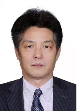 Yuanfu Zhao (赵元富)合作论文数School of Electronics and Information Engineering, Hangzhou Dianzi University2
 Lei Shu (舒磊)合作论文数College of Artificial Intelligence, Nanjing Agricultural University;NAU-Lincoln Joint Research Center of Intelligent Engineering;Beyond Intelligent Phytoprotection Research Institute, Nanjing Agricultural University;School of Engineering, College of Health and Science, University of Lincoln2Dongqiang Li合作论文数1Dan Wang合作论文数1




