A separate absorption, charge, and multiplication In/sub 0.53/Ga/sub 0.47/As-In/sub 0.52/Al/sub 0.48/As avalanche photodiode with an impact-ionization-engineered multiplication region is reported. By implementing an electric field gradient in the multiplication region, better control of impact-ionization can be achieved. Gain-bandwidth product of 160 GHz and excess noise factor with an equivalent k value of 0.1 are demonstrated.
We identify a new shot noise suppression mechanism in a thin (~100 nm) heterostructure avalanche photodiode. In the low-gain regime the shot noise is suppressed due to temporal correlations within amplified current pulses. We demonstrate in a Monte Carlo simulation that the effective excess noise factors can be <1, and reconcile the apparent conflict between theory and experiments. This shot noise suppression mechanism is independent of known mechanisms such as Coulomb interaction, or reflection at heterojunction interfaces.
A dark count rate in InP-based single photon counting avalanche photodiodes is a limiting factor to their efficacy. The temperature dependence of the dark count rate was studied to understand its origin in In0.53Ga0.47As∕In0.52Al0.48As separate-absorption-charge-multiplication avalanche photodiodes. The dark count rate was observed to be a very weak function of temperature in the range from 77Kto300K. Various mechanisms for dark count generation were considered. Simulations of band-to-band tunneling in the In0.52Al0.48As multiplication layer were found to agree well with the experimental temperature dependence of dark count rate at various excess biases. To reduce tunneling-induced dark counts, a suitable design change to the detector structure is proposed.
This study demonstrates 1.52 /spl mu/m Geiger mode operation of an In/sub 0.53/Ga/sub 0.47/As/In/sub 0.52/Al/sub 0.48/As APD. A study of the origin of dark count rate in this detector is also presented.
We report avalanche photodiodes with a "centered-well" multiplication region that have achieved high gain, low noise, and low dark current. The multiplication region consists of an similar to 80 nm-thick Al0.2Ga0.8As layer sandwiched between two thin (10 similar to 20 nm) layers of Al0.6Ga0.4As. Monte Carlo simulation shows the beneficial effect of spatial modulation of the ionization rates in this structure compared to homojunctions.
We present a Monte. Carlo simulation of the bandwidth of an InAIAs avalanche photodiode with an undepleted absorber. The carrier velocities are simulated in the charge layer and the multiplication region. It is shown that the velocity overshoot effect is not as significant as simpler models have suggested. At high electric field intensity, the electron effective saturation velocity is only slightly higher when impact ionization is significant, compared with when impact ionization is absent. The simulated 3 dB bandwidth is consistent with experiments for gains up to 50.
We report an avalanche photodiode with an undepleted p-type InGaAs absorption region and a thin InAlAs multiplication layer. The motivation for utilizing an undepleted absorption layer, which is similar to that in the unitraveling carrier photodiode, is to reduce the dark current. A dark current below 1 nA at a gain of 10 and a gain–bandwidth product of 160 GHz are demonstrated.
Low-temperature photon counting with gated mode quenching is demonstrated with separate absorption, charge, and multiplication avalanche photodiodes that have an In0.52Al0.48As multiplication layer. A minimum of ten dark counts per second and single-photon detection efficiency of 16% were achieved at 130 K.
Monte Carlo simulations of Hg0.7Cd0.3Te avalanche photodiodes are presented. The simulated very low excess noise and exponential gain curve are consistent with those that have been experimentally observed and are consistent with the speculated large ratio of electron and hole impact ionization rates. The simulations suggest that there is a large difference between the scattering rates of electrons and holes, a direct consequence of the band structure. A resonance behavior in the excess noise factor at gain values near 2, 4, 8, and 16 is also revealed in the simulations. This effect is explained by comparing to the gain and noise of a photomultiplier tube.
Low-temperature photon counting with gated mode quenching is demonstrated with separate absorption, charge, and multiplication avalanche photodiodes that have an In/sub 0.52/Al/sub 0.48/As multiplication layer. A minimum of ten dark counts per second and single-photon detection efficiency of 16% were achieved at 130 K.
The breakdown probabilities of avalanche photodiodes (APDs) working in the Geiger mode are analyzed using a history-dependent analytical impact-ionization model [R. J. McIntyre, IEEE Trans. Electron Devices 46, 1623 (1999)]. The breakdown sharpness in devices with thin and thick multiplication regions is found to follow the same trend in GaAs, InAlAs, and InP material systems. Breakdown characteristics of InP and InAlAs are compared for their applications in photon counting at telecommunication wavelengths.
This paper surveys recent work in several photodetector areas including high-speed, low-noise avalanche photodiodes, solar-blind ultra-violet PIN photodiodes, and quantum dot infrared photodetectors (QDIPs).
Al x Ga 1−x As (x=0.0–0.9) homojunction avalanche photodiodes are characterized in the temperature range of 11–300 K. For all compositions, the breakdown electric field strength decreases with temperature, and the rate of change is smaller at temperatures below 50 K than at higher temperatures. This results from the fact that spontaneous phonon emission dominates carrier scattering in the 0 K limit. The rate of change of the breakdown field strength is smallest for Al0.6Ga0.4As compared with other compositions. This is likely due to higher alloy scattering at x=0.6. A Monte Carlo model that provides good fits to experimental data is presented.
It is well known that, as a result of the nonlocal nature of impact ionization, the noise of avalanche photodiodes decreases as the thickness of the multiplication region is reduced. In this paper, we present an alternative technique to calculate the gain distribution, including the dead-space effect, by numerical solution of the recursive equations. This method yields the average gain, the multiplication noise, and gain distribution curves. The results are compared with simple Monte Carlo simulation and the Z-transform technique.
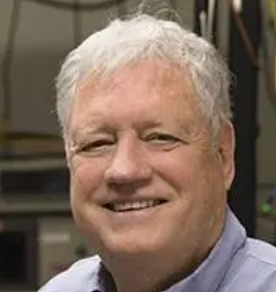 Joe Charles Campbell合作论文数School of Engineering and Applied Science, University of Virginia20
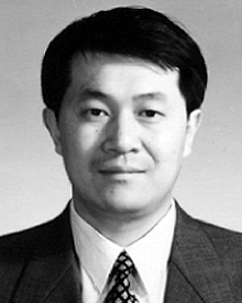 Xiaoguang Zheng合作论文数Electrical and Computer Engineering Department, University of Virginia15
 Shuling Wang合作论文数Microelectronics Research Center;Department of Electrical and Computer Engineering;University of Texas at Austin;Microelectronics Research Center, University of Texas at Austin12
 Gauri Karve合作论文数12
 Archie L. Holmes Jr.合作论文数Chandra Department of Electrical and Computer Engineering, Cockrell School of Engineering, University of Texas at Austin11
 Ning Li (李宁)合作论文数8Xw Li合作论文数7Sw Xia合作论文数6
 Xiaoguang Sun (孙晓光)合作论文数6Rubin Sidhu合作论文数6William P. Risk合作论文数5Isshiki Takahiro合作论文数5
 Geoffrey S. Kinsey合作论文数Spectrolab , Inc5
 Joseph Boisvert合作论文数5
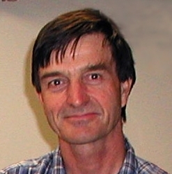 Donald S. Bethune合作论文数IBM Almaden Research Center5Rengarajan Sudharsanan合作论文数5
 S. Wang合作论文数4
 Xiaowei Li (李晓维)合作论文数University of Chinese Academy of Sciences;State Key Lab of Computer Architecture, Institute of Computing Technology, Chinese Academy of Sciences4Xiaofeng Zhang合作论文数4
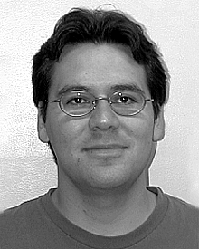 Jeffrey B. Hurst合作论文数4
 Larry A. Coldren合作论文数Optoelectronics Technology Center, Department of Electrical & Computer Engineering, College of Engineering, University of California, Santa Barbara4
 Hui Su合作论文数Fidelity Investments3
 Andrew S. Huntington合作论文数3
 Zesheng Tang (唐泽圣)合作论文数Space Science Institute, Macau University of Science and Technology2A. Holmes合作论文数2Wai Wan Tsang合作论文数2Shaowei Xia (夏绍玮)合作论文数2Joe C. Campbell合作论文数2MA KINCH合作论文数1Et Kim合作论文数1
 Chang-Feng Wan合作论文数1Bin Zhao (赵斌)合作论文数1Xin Li合作论文数1Ning Duan合作论文数1Zhonghui Chen合作论文数1Wen Ping Wang合作论文数1
 Xiaoli Sun合作论文数Goddard Space Flight Center, National Aeronautics and Space Administration1
 Anupam Madhukar合作论文数The Mork Family Department of Chemical Engineering and Materials Science, School of Engineering, University of Southern California;Alfred E. Mann Department of Biomedical Engineering, School of Engineering, University of Southern California;Ming Hsieh Department of Electrical and Computer Engineering, School of Engineering, University of Southern California1Bing Yang合作论文数1Xiaoping Li合作论文数1Wei Shi (石伟)合作论文数1
 Wenping Wang合作论文数Department of Computer Science & Engineering, College of Engineering, Texas A&M University1M. M. Wong合作论文数1A. L. Beck合作论文数Microelectronics Research Center, The University of Texas at Austin1
 Uttiya Chowdhury合作论文数School of Electric and Computer Engineering, Georgia Institute of Technology1
 Chad S. Wang合作论文数1Stephane Demiguel合作论文数1Yilong Liang合作论文数1




