Solvent-resistant nanofiltration (SRNF) has emerged as a promising alternative to conventional distillation for removing impurities, recovering solutes, and regenerating solvents from diluted process streams. For most industries, such as the pharmaceutical and (petro)chemical industry, the key important factor here is energy-efficiency gain. This study investigates the physicochemical properties of metalcone hybrid layers, such as layer thickness, composition, and layer-solvent interactions. It also utilizes surface-silanization to increase the hydrophobicity of these layers, grown on both planar silicon and 3D-porous ceramic substrates. Using the molecular layer deposition (MLD) technique, vapor-phase titanium tetra-chloride and trimethyl-aluminum are employed as precursors, with ethylene glycol as a co-reactant for nanopore fabrication and methyltrimethoxysilane for surface-silanization. MLD layers were deposited at 125°C and 150°C, followed by annealing in air and nitrogen (N2) at 250°C and 350°C. The resulting SRNF membranes demonstrated high chemical stability in polar and non-polar solvents, as well as in water-solvent mixtures, maintaining permeation rates after 48 hours of continuous exposure. Furthermore, after surface-silanization and enhanced hydrophobicity, the n-hexane permeance was tripled for surface-silanized titanicone and doubled for alucone hybrid layers compared to the unsilanized hybrid layers. Conversely, demineralized water permeance decreased. The SRNF membranes, with pore diameters of <2 nm, show a >90% rejection for polyethylene glycol molecular sizes >390 Dalton. The final n-hexane permeance of surface-silanized, air- and N2-annealed metalcone hybrid layer membranes was >10 L·m⁻2·hr⁻1·bar⁻1. These results demonstrate the versatility of MLD as a technology ready for further developing membranes towards large-scale industrial applications.
Atomic layer etching (ALE) has emerged as a transformative technique for achieving atomic and close-to-atomic scale manufcturing, addressing the critical challenges in scaling, three-dimensional (3D) integration, and defect management inherent to advanced nanofabrication. Built on decades of advancements in plasma processing and atomic layer deposition (ALD), ALE is a self-limiting and cyclic process that enables unparalleled control over the etch depth resolution, surface smoothness, and material selectivity. In this review, the underlying chemical and physical mechanisms of ALE are outlined, with focus on the reaction dynamics at plasma–surface interfaces, defect-sensitive chemistry, and synergistic integration with ALD. Recent technological advancements are highlighted through case studies, demonstrating the capacity of ALE for selective material removal in heterogeneous systems, precise control of the surface morphology in high-aspect-ratio structures, and deterministic 3D nanopatterning for emerging architectures. This review further explores the unique role of ALE in cutting-edge fields such as extreme manufacturing and constructs a system logic framework spanning computational simulation and mechanisms to future applications, highlighting ALE as a driving force for the strategic development of future multi-domain technology. Current challenges are critically examined, and forward-looking perspectives are provided, indicating the potential of ALE as a cornerstone in the fabrication of next-generation semiconductors. By integrating fundamental mechanistic insights with industrial strategies, this review bridges theoretical understanding and practical applications while charting a roadmap for advancing ALE as a transformative approach to atomic-precision manufacturing.
Molecular layer deposition is increasingly used to functionalize the surface of planar and 3D porous substrates. This study explores functionalized 'alucone' hybrid layers grown on ceramic substrates to enhance their surface hydrophobicity. The layers were made from trimethyl-aluminum as a precursor with five different alcohols as a co-reactant: aliphatic (ethane-1,2-diol, 2,2-oxydiethanol, 1,6-hexanediol), and aromatic (4-aminophenol, benzene-1,4-diol). After post-deposition annealing in N2 atmosphere at 250 and 350(degrees)C, the changes in the physical properties and the chemical affinity of the layers were studied and compared to those of the as-deposited hybrid layers. Differential thermal analysis of the hybrid layers showed higher decomposition temperatures for the layers grown from aromatic alcohols than for those grown from aliphatic alcohols. Additionally, Fourier- transform infrared and X-ray photoelectron spectroscopy showed that an increase in annealing temperature decreased the concentrations of surface hydroxyl-groups and caused changes in the carbon-related groups. These results could be correlated to the hydrophobicity of the layers: higher water contact angles (>90(degrees)) were measured for annealed samples, compared to those (<90(degrees)) of the as-deposited samples grown at 150(degrees)C. These findings confirm that the proposed method of MLD functionalization and post-deposition annealing can be used to tune the surface hydrophobicity of ceramic membranes.
Ceramic membrane technology, whether applied as a stand-alone separation technology or in combination with energy-intensive approaches like distillation, is a promising solution for lower energy alternatives with minimal carbon footprints. To improve the separation of solutes in the nanofiltration range from industrial wastewater streams, ceramic nanofiltration (NF) membranes with reproducible sub-nanometre pore sizes are required. To achieve this, the emerging technique of molecular layer deposition (MLD) is employed to develop ceramic NF membranes, and its efficiency and versatility make it a powerful tool for preparing uniform nanoscale high-porosity membranes. Our work, which involved vapor-phase titanium tetrachloride as a precursor and ethylene glycol as a co-reactant, followed by calcination in air at 350 °C, resulted in NF membranes with pore sizes (radii) around ~0.8 ± 0.1 nm and a demineralized water permeability of 13 ± 1 L·m−2·h−1·bar−1.The high-water flux with >90% rejection of polyethylene glycol molecules with a molecular size larger than 380 ± 6 Dalton indicates the efficiency of the MLD technique in membrane functionalization and size-selective separation processes, and its potential for industrial applications.
The history of Atomic Layer Deposition (ALD) has been extensively researched in the VPHA-project (www.vph-ald.com/) initiated in 2013 by R. Puurunen [1]. It is commonly accepted that Atomic Layer Deposition (ALD) was conceived in the Baltic area as a unique ultrathin-film growth method based on the repeated, self-terminating gas-solid half-reactions of at least two volatile compounds on a solid substrate surface. Originally, in the 1960’s, the Russians Alekskovski and Kol'tsov [2]) named this method Molecular Layering and exactly 50 years ago, in 1974 the Finnish inventors Suntola and Antson [3] patented the method as Atomic Layer Epitaxy. This fact has been officially celebrated at the 24th ALD Conference in Helsinki (Aug. 5, ’24 ald2024.avs.org). Atomic Layer Etching (ALE) has lagged behind ALD. For long [4,5] the first patent published on ALE was thought to have been initiated by Max Yoder [6]. In 1987 he conceived the idea on diamond etching with intermittent pulsing of nitrogen dioxide and noble gas ions mixed with hydrogen gas. However, it was Seiichi Iwamatsu (Fig. 1) of Seiko Epson, Japan, who filed in 1981 an application on Si-etching by repeated exposure to iodine (I2) chemistry at moderate temperatures (20 °C to 100 °C) followed by a light or heat pulse up to ~ 300 °C [7]; see Fig. 2. This patent was followed by several others on ALE [8]. One of these patents disclosed quasi-ALE (named “digital etching”) via Si-surface modification by “lamination” of a single Cl-atomic layer from exposure to Cl2 gas, followed by a removal step carried out by Ar+-ion bombardment to etch off “one atomic layer or at most three atomic layers by controlling the kinetic energy” [9]. This presentation will highlight the groundbreaking work and background of the Japanese inventor Seiichi Iwamatsu. Born in 1939 in Kyoto to a family of doctors - his father being a practicing physician- he grew up and studied in Osaka, after which he spent many years as a ‘master inventor’ (over 1200 patents filed in his name) for Seiko Epson (~1970-1990) and others afterwards. He played key roles in thin-film technology and e-beam lithography. He also contributed to the success story of Seiko’s quartz watch, a masterpiece in micromachining a miniature tuning fork from crystalline fused silica, tuning/trimming it to 32,768 Hz (=215 Hz), packaging it in a hermetically sealed case and integrating it with flip-flop frequency dividing and counting electronic circuitry and a step motor [10]. From the above it is clear that Mr. Iwamatsu can be recognized as the original inventor of Atomic Layer Etching. ---------------------------------------------------- Acknowledgement The authors would like to thank Dr. Masanobu Honda (Tokyo Electron Miyagi Ltd., Japan) for his support in retrieving some of the historic facts mentioned herewith about Dr. Iwamatsu. References [1] R.L. Puurunen, Chem. Vap. Deposition 20, pp. 332–344 (2014); doi:10.1002/cvde.201402012. [2] V.B. Alekskovski and S. I. Kol'tsov, Some characteristics of molecular layering reactions, Abstract of Scientific and Technical Conference, Goskhimizdat, Leningrad, 1965, p. 67 (in Russian). [3] T. Suntola and J. Antson, FIN 52359, priority Nov. 29, 1974, US Patent 4,058,430, Nov. 15, 1977. [4] K.J. Kanarik, et al., J. Vac. Sci. Technol. A33, 020802 (2015); doi/10.1116/1.4913379. [5] W.M.M. Kessels, www.atomiclimits.com/ March 2, 2020. [6] M.N. Yoder, Atomic Layer Etching, US Patent 4,756,794, July 12, 1988; assigned to US Navy. [7] S. Iwamatsu, Atomic Layer Etching Method, JPS5898929A / JPH0379862B2; priority Dec. 9, 1981, published June 13, 1983; assigned to Seiko Epson Corp. [8] https://worldwide.espacenet.com/patent/search/family/016189802/publication/JPH0472726A?q=iwamatsu%20seiichi%20atomic%20layer%20etching [9] S. Iwamatsu, Digital Etching Process, JPH0472726A, priority: July 13, 1990, published March 6, 1992; assigned to Seiko Epson Corp. [10] https://corporate.epson/en/technology/search-by-products/wearable/quartz-watch.html Figure 1
Atomic layer deposition (ALD) is known for its unparalleled control over layer thickness and 3D conformality and could be the future technique of choice to tailor the pore size of ceramic nanofiltration membranes. However, a major challenge in tuning and functionalizing a multichannel ceramic membrane is posed by its large internal pore volume, which needs to be evacuated during ALD cycling. This may require significant energy and processing time. This study presents a new reactor design, operating at atmospheric pressure, that is able to deposit thin layers in the pores of ceramic membranes. In this design, the reactor wall is formed by the industrial tubular ceramic membrane itself, and carrier gas flows are employed to transport the precursor and co-reactant vapors to the reactive surface groups present on the membrane surface. The layer growth for atmospheric-pressure ALD in this case proceeds similarly to that for state-of-the-art vacuum-based ALD. Moreover, for membrane preparation, this new reactor design has three advantages: (i) monolayers are deposited only at the outer pore mouths rather than in the entire bulk of the porous membrane substrate, resulting in reduced flow resistances for liquid permeation; (ii) an in-line gas permeation method was developed to follow the layer growth in the pores during the deposition process, allowing more precise control over the finished membrane; and (iii) expensive vacuum components and cleanroom environment are eliminated. This opens up a new avenue for ceramic membrane development with nano-scale precision using ALD at atmospheric pressure.
Area-selective atomic layer deposition (AS-ALD) processes for TiO2 and TiON on SiN as the growth area vs SiO2 as the nongrowth area are demonstrated on patterns created by state-of-the-art 300 mm semiconductor wafer fabrication. The processes consist of an in situ CF4/N2 plasma etching step that has the dual role of removing the SiN native oxide and passivating the SiO2 surface with fluorinated species, thus rendering the latter surface less reactive toward titanium tetrachloride (TiCl4) precursor. Additionally, (dimethylamino)trimethylsilane was employed as a small molecule inhibitor (SMI) to further enhance the selectivity. Virtually perfect selectivity was obtained when combining the deposition process with intermittent CF4/N2 plasma-based back-etching steps, as demonstrated by scanning and transmission electron microscopy inspections. Application-compatible thicknesses of ∼8 and ∼5 nm were obtained for thermal ALD of TiO2 and plasma ALD of TiON.
Atmospheric-pressure plasma-enhanced spatial atomic layer deposition (PE-spatial-ALD) of SiNx is demonstrated for the first time. Using bis(diethylamino)silane (BDEAS) and N2 plasma from a dielectric barrier discharge source, a process was developed at low deposition temperatures (≤ 250 °C). The effect of N2 plasma exposure time and overall cycle time on layer composition was investigated. In particular, the oxygen content was found to decrease with decreasing both above-mentioned parameters. As measured by depth profile X-ray photoelectron spectroscopy, 4.7 at.% was the lowest oxygen content obtained, whilst 13.7 at.% carbon was still present at a deposition temperature of 200 °C. At the same time, deposition rates up to 1.5 nm/min were obtained, approaching those of plasma enhanced chemical vapor deposition and thus opening new opportunities for high-throughput atomic-level processing of nitride materials.
Atomic layer deposition (ALD) is a widely recognized technique for depositing ultrathin conformal films with excellent thickness control at Ångström or (sub)monolayer level. Atmospheric-pressure ALD is an upcoming ALD process with a potentially lower ownership cost of the reactor. In this review, we provide a comprehensive overview of the recent applications and development of ALD approaches emphasizing those based on operation at atmospheric pressure. Each application determines its own specific reactor design. Spatial ALD (s-ALD) has been recently introduced for the commercial production of large-area 2D displays, the surface passivation and encapsulation of solar cells and organic light-emitting diode (OLED) displays. Atmospheric temporal ALD (t-ALD) has opened up new emerging applications such as high-porosity particle coatings, functionalization of capillary columns for gas chromatography, and membrane modification in water treatment and gas purification. The challenges and opportunities for highly conformal coating on porous substrates by atmospheric ALD have been identified. We discuss in particular the pros and cons of both s-ALD and t-ALD in combination with their reactor designs in relation to the coating of 3D and high-porosity materials.
Since G. Moore’s historical observation [1] that the functionality per chip (bits, transistors) as well as MPU performance (clock frequency in MHz × instructions per clock = millions of instructions per second) doubles every 1.5 to 2 years, the semiconductor industry has continued to grow to over 600 G$ in 2022 [2]. The IRDS 2022 Roadmap [3] catches the scaling challenges faced for the upcoming decades by the term ‘3D Power Scaling’. This period is the third in a sequence of eras that started early on with straightforward geometrical scaling by continuous shortening of the wavelengths (from regular UV to deep UV/immersion) used in the lithographic patterning of planar transistor structures (Fig. 1a). In the second, almost past ‘equivalent scaling’ era, new superior material properties and critical dimensions nearing single-digit nanometer values could still be realized by cost-effective technology solutions, often in spite of the delay in (EUV) lithography solutions. Ever more complex device architectures requiring extreme edge placement accuracy, layer conformality and shape fidelity in all processing steps (deposition, etching) could be fully 3D-integrated into vertical intra- and inter-chip concepts (Fig. 1b) thus alleviating the need for new capital-intensive lithography tools capable of higher resolution (~ 40% of total tool costs). Figure 2 illustrates the development in the past 65 years of the non-lithographic technologies that have sustained Moore’s Law , as driven by continuous downscaling of CMOS devices. Two extra trends have set in half way (~1993): single-wafer processing and heterogeneous device integration. The latter development, often coined as More than Moore , a term that was introduced in the 2005 ITRS Roadmap, and refers to the silicon-compatible integration of devices with functionalities that do not necessarily scale according to Moore's Law, but provide additional value in different ways. The More-than-Moore approach allows for the incorporation of non-digital functionalities ( e.g ., RF communication, passive components, power control, sensors, actuators) that can flexibly move from the system board-level into the package (SiP) or onto the chip (SoC). We will discuss a kaleidoscopic view of the author’s activities in Rapid Thermal Processing, RIE etching for TSVs, RF-SIP integration of passives, and Atomic Layer Processing (deposition, etch, and cleaning). In sub-10 nm scaling and fabrication of 3D architectures, especially the techniques of ALD and ALE have manifested to cost-effectively bridge the record incubation time needed to bring EUV technology from prototype to commercial use. More importantly, these unique techniques can be used to create advanced devices in dedicated isotropic (thermal and radical-enhanced) and anisotropic (directional and ion-enhanced) processing modes. Here, energetic species (radicals and/or ions in a plasma) are used in one or two steps, with the ions yielding anisotropic profiles (used in FinFET logic and 3D NAND memory), and neutrals and radicals yielding isotropic profiles used to deposit or etch the features in horizontal nanowires, nanosheets and ‘forksheets’ in GAA-FETs. 1. G. Moore, Cramming more components onto integrated circuits, Electronics 38 (8), (1965) 114-118. 2. https://www.semiconductors.org/global-semiconductor-sales-increase-24-year-to-year-in-october-annual-sales-projected-to-increase-26-in-2021-exceed-600-billion-in-2022/ 3. International Roadmap for Devices and Systems (IRDS™) 2022 Edition - IEEE IRDS™. Fig. 1. a) Different scaling ages for device manufacturing; b) the planar-to-GAA transition; after [3]. Fig. 2. Historic and future perspectives of non-lithographic key technologies in IC scaling. Figure 1
A first-of-its-kind area-selective deposition process for SiO2 is developed consisting of film deposition with interleaved exposures to small molecule inhibitors (SMIs) and back-etch correction steps, within the same spatial atomic layer deposition (ALD) tool. The synergy of these aspects results in selective SiO2 deposition up to ~23 nm with high selectivity and throughput, with SiO2 growth area and ZnO nongrowth area. The selectivity is corroborated by both X-ray photoelectron spectroscopy (XPS) and low-energy ion scattering spectroscopy (LEIS). The selectivity conferred by two different SMIs, ethylbutyric acid, and pivalic acid has been compared experimentally and theoretically. Density Functional Theory (DFT) calculations reveal that selective surface functionalization using both SMIs is predominantly controlled thermodynamically, while the better selectivity achieved when using trimethylacetic acid can be explained by its higher packing density compared to ethylbutyric acid. By employing the trimethylacetic acid as SMI on other starting surfaces (Ta2 O5 , ZrO2 , etc.) and probing the selectivity, a broader use of carboxylic acid inhibitors for different substrates is demonstrated. It is believed that the current results highlight the subtleties in SMI properties such as size, geometry, and packing, as well as interleaved back-etch steps, which are key in developing ever more effective strategies for highly selective deposition processes.
Area-selective atomic layer deposition (AS-ALD) holds great potential for advancing device manufacturing. 1 Recently, outstanding progress on this topic has been made in terms of understanding and developing highly selective processes for various material systems; some of these processes have already been transferred into fabs. 2 In this work we provide an overview of AS-ALD of silicon-based materials with high selectivity and high throughput, especially silicon oxide and nitride. While the selectivity is mostly governed by the method of choice and the underpinning chemistry, the aspect of high-throughput is ensured by using spatial ALD, which is, in our case, performed at atmospheric pressure. The processes presented here comprise three steps: selective inhibitor chemisorption, plasma-based spatial ALD and spatial back-etching. Particular focus is given to the choice of inhibitors as the most critical step in enabling high-selectivity. Here, density functional theory (DFT) calculations have been employed to unveil the chemistries governing the selectivity for the two different inhibitors within the same growth system. General guidelines on the inhibitor chemistries are derived by combining experimental and DFT results. Finally, process details and effect of plasma chemistries on different surfaces are discussed in an effort to expand the selectivity toolbox to other silicon-based materials. [1] A. Mameli, et al ., “ Area-Selective Atomic Layer Deposition of SiO 2 using acetylacetone as a chemoselective inhibitor in an ABC-type cycle”, ACS Nano , 11 , 9303, 2017. [2] H.-P. Chen, , et al. , “Fully Self-Aligned Via Integration for Interconnect Scaling Beyond 3nm Node” , IEDM 2021, paper 22-1. Figure 1
An atmospheric-pressure plasma-enhanced spatial atomic layer deposition (PE-s-ALD) process for SiO2 using bisdiethylaminosilane (BDEAS, SiH2[NEt2]2) and O2 plasma is reported along with an investigation of its underlying growth mechanism. Within the temperature range of 100-250 °C, the process demonstrates self-limiting growth with a growth per cycle (GPC) between 0.12 and 0.14 nm and SiO2 films exhibiting material properties on par with those reported for low-pressure PEALD. Gas-phase infrared spectroscopy on the reactant exhaust gases and optical emission spectroscopy (OES) on the plasma region are used to identify the species that are involved in the ALD process. Based on the identified species, we propose a reaction mechanism where BDEAS molecules adsorb on -OH surface sites through the exchange of one of the amine ligands upon desorption of diethylamine (DEA). The remaining amine ligand is removed through combustion reactions activated by the O2 plasma species leading to the release of H2O, CO2, and CO in addition to products such as N2O, NO2, and CH-containing species. These volatile species can undergo further gas-phase reactions in the plasma as indicated by the observation of OH*, CN*, and NH* excited fragments in OES. Furthermore, the infrared analysis of the precursor exhaust gas indicated the release of CO2 during precursor adsorption. Moreover, this analysis has allowed the quantification of the precursor depletion yielding values between 10 and 50% depending on the processing parameters. Besides providing insights into the chemistry of atmospheric-pressure PE-s-ALD of SiO2, our results demonstrate that infrared spectroscopy performed on exhaust gases is a valuable approach to quantify relevant process parameters, which can ultimately help evaluate and improve process performance.
The combination of area-selective ALD intermitted with back-etching steps has recently attracted much interest because of its potential in achieving high selectivity. Compared to non-interrupted area-selective ALD this supercycle approach has proven to be very effective in reducing the defectivity on the non-growth areas and thickening the layers on the growth areas.1, 2 In this work we studied the case of selective SiO2 deposition on silicon substrate wafers (growth area) with large ZnO patterns (non-growth area). We will demonstrate the effectiveness of this complementary approach, i.e., deposition and etch-back corrections in a rotary atmospheric-pressure all-spatial processing (= ‘dep/etch’) reactor (Fig. 1) to maximize SiO2 selectivity while obtaining high deposition rates. For the selective spatial ALD part of the supercycle a three-step (‘ABC’-type) recipe was adopted,3 consisting of exposure to: A) inhibitor, B) silicon precursor (BDEAS) and C) O2 plasma. The periodic back-etch intermissions in the supercycle were carried out in the same integrated spatial process reactor by exposing the substrate to a CF4-O2-N2 plasma. The plasma source used for both O2-plasma and the back-etch was of the atmospheric-pressure Dielectric Barrier Discharge (DBD) type4. Figure 2 gives an illustration for a supercycle process with the substrate rotating at 20 rpm and using 3 repetitions of 40 ‘ABC’-cycles and 6 corrective back-etch cycles. During the each set of 40 ‘ABC’-cycles we could selectively grow sufficient (i.e., up to ~3.5 nm) SiO2 layer thickness on the growth area before the first nucleation of SiO2 became apparent on the ZnO non-growth areas. This way some selectivity is gradually lost with the number of ALD cycles increasing. As shown in Fig. 2 the selectivity loss can be repeatedly restored by a CF4-O2-N2 plasma back-etch with no silicon detected on the non-growth area by XPS. We demonstrated that with 3 repeated ‘dep/etch’ supercycles up to 10 nm thick SiO2 could be grown on the growth area. We will discuss how Low Energy Ion Spectroscopy (LEIS), with its extreme sensitivity to the top monolayer(s) of a thin film, can give more and reliable quantitative information on the process selectivity and the defectivity on the non-growth area in terms of surface coverage and derived thickness. In addition, scanning probe FTIR-AFM microscopy can give information about the defects and contaminants at the substrate surface. Furthermore, we extended the selective spatial ALD of SiO2 to other oxidic non-growth areas like Al2O3, IGZO, SnO2, Ta2O5 and ZrO2. 1. R. Vallat, et al., J. Vac. Sci. Technol. A, 35, 01B104 (2017). 2. S. K. Song, et al., Chem. Mater. 31, 4793-4804 (2019). 3. A. Mameli, et al., ACS Nano, 11, 9303-9311 (2017). 4. Y. Creyghton, P. Poodt, M. Simor, F. Roozeboom, US Patent Application 20170137939. Figure 1
Today, Li-ion batteries are key devices in energy storage, with a wide set of applications ranging from mW to kW, such as portable electronics devices, electric vehicles and grid-storage. Typically, high energy density anodes such as Si or Li, combined with Ni- or Li-rich cathodes 1,2 are necessary to obtain the targeted gravimetric energy density (>350 Wh/kg). However, several high-potential redox-chemistries can lead to serious safety and degradation issues during charge-discharge cycling due to oxidative and reductive instabilities 3, that often occur at the electrode-electrolyte interfaces 4. Therefore, for every Li-ion battery chemistry the optimization of these interfaces with chemo-mechanically stable and Li-ion conductive passivation layers is essential in mitigating the non-compatibility of the individual cell components. These interface stabilizing layers can be incorporated either in-situ by using electrolyte additives or ex-situ by chemical and physical methods. One popular option here is offered by atomic layer deposition (ALD) which is today’s technology of choice to achieve films with superior quality and 3D-conformality with atomic-scale thickness precision. However, conventional vacuum-based temporal ALD is not compatible with industrial high-throughput roll-to-roll battery electrode production. Here, the technique of large-area atmospheric-pressure spatial-ALD (s-ALD) as pioneered by TNO-Holst Centre over a decade ago can offer prime solutions for various applications including thin-film batteries 5. This technique opens up a wide range of cost-effective applications based on materials like metal oxides, nitrides, sulfides, oxysulfides as well as hybrid organic-inorganic material combinations. In this presentation, we will discuss the growth of several s-ALD films made from Al2O3, TiO2, and ZnO which have been specifically optimized for dendritic Li-growth suppression, interface stabilization, and cathode degradation protection. Next, we will discuss some recent results on the up-scalable s-ALD growth of thin LiPON electrolyte films with a high Li-ion conductivity of >10-7 S/cm, low electronic conductivity of <10-12 S/cm, and high stability against anodic Li-metal during cycling. This electrolyte is also essential in the development of protective layers in liquid and polymer electrolyte-based Li-ion batteries, and in thin-film solid-state batteries with ultra-thin electrolyte layers and planar and 3D topologies. REFERENCES S. Myung et al., ACS Energy Lett. 2, 196–223 (2017). G. Assat and J. M. Tarascon, Nat Energy 3, 373–386 (2018). H. Ryu et al., Chem. Mater. 3 (30), 1155-1163 (2018). D. Aurbach et al., Solid State Ionics 148, 405–416 (2002). P. Poodt et al., J. Vac. Sci. and Technol. A 30, 010802 (2012).
Area-selective ALD interleaved with etch-back steps in a supercycle fashion has recently been reported as very effective in achieving high selectivity. Such supercycles can result in lower defectivity on the non-growth area and thicker layers on the growth area, as compared to solely area-selective ALD.1, 2 Here, we use low energy ion scattering (LEIS) to probe the selectivity of the first supercycle, consisting of plasma-enhanced selective spatial-ALD of SiO2 and conventional CF4-based reactive ion etching (RIE). Given its extreme sensitivity to the top monolayer(s) of a thin film, LEIS can reliably quantify the selectivity/defectivity on the non-growth areas in terms of surface coverage and derived thickness. A three-step approach was used for the area-selective spatial ALD of SiO2,3 which consisted of inhibitor, silicon precursor (BDEAS), and O2 plasma exposures. The process selectivity as a function of the number of cycles was probed using LEIS to monitor the SiO2 surface coverage on the non-growth area. After 20 spatial ALD cycles, no silicon was detected on the non-growth area (detection limit 2 % SiO2 surface coverage), implying excellent process selectivity. Increasing the number of ALD cycles resulted in a gradual loss of selectivity. Interestingly after 110 ALD cycles, the SiO2 coverage was 86%, indicating a not yet closed layer. At the same time, a SiO2 thickness of 11 nm was measured on the growth area, using spectroscopic ellipsometry. As the last step of the super-cycle, a 3 seconds RIE was sufficient to bring the SiO2 coverage back to zero on the non-growth area, while an 8 nm thick SiO2 layer was left on the growth area. The data presented in this work demonstrate the effectiveness of combining area-selective spatial ALD + etch-back corrections to achieve extreme SiO2 selectivity while retaining high deposition rates. Finally, we have extended the plasma-enhanced area-selective spatial ALD of SiO2 to other oxides and metals non-growth areas. REFERENCES 1. R. Vallat et al., JVSTA, 35, 01B104 (2017). 2. S. K. Song et al., Chem. Mater. 31 4793-4804 (2019). 3. A. Mameli et al., ACS Nano, 11, 9303-9311 (2017). Figure 1
Welcome to G01: Atomic Layer Deposition Applications 16! Take a moment to listen to welcome remarks from the lead organizer, Fred Roozeboom.
 Paul Poodt合作论文数39
 Klootwijk Johan H合作论文数37
 Richard Sanden合作论文数Department of Applied Physics, Eindhoven University of Technology;Dutch Institute for Fundamental Energy Research29
 Verheijen Marcel A合作论文数Dept Appl Phys, Eindhoven Univ Technol27
 Erwin Kessels合作论文数Eindhoven Institute for Renewable Energy Systems, Eindhoven University of Technology;Department of Applied Physics and Science Education, Eindhoven University of Technology;ALD Academy;AtomicLimits.com27Illiberi Andrea合作论文数Dipartimento di Fisica;Studi di Milano;Dipartimento di Fisica, Studi di Milano25A. Mameli合作论文数23
 Jinesh K. B合作论文数Kamerlingh Onnes Laboratory;Leiden University;Kamerlingh Onnes Laboratory, Leiden University21W Besling合作论文数17
 Y. Lamy合作论文数LETI, MINATEC Campus17
 Raymond Duffy合作论文数Tyndall National Institute, University College Cork;School of Engineering, University College Cork13
 Erik Langereis合作论文数13w dekkers合作论文数12
 A.J.M. Mackus合作论文数11
 Peter H. L. Notten合作论文数Institute of Energy and Climate Research, Forschungszentrum Jülich11Thuy Dao合作论文数10Eva Tois合作论文数10
 Harm C. M. Knoops合作论文数10Jgm Van Berkum合作论文数9a kemmeren合作论文数9s b s heil合作论文数9J.G.M Van Berkum合作论文数9
 Bora Karasulu合作论文数Department of Chemistry, Faculty of Science, Engineering and Medicine, The University of Warwick8
 Valentino Longo合作论文数8
 Jonas Sundqvist合作论文数Qimonda Dresden GmbH & Co. OHG8
 Monja Kaiser合作论文数8Nick Cowern合作论文数8Yves Creyghton合作论文数7F. van den Bruele合作论文数7Pa Stolk合作论文数7Kristína Hušeková合作论文数7
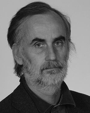 Karol Frohlich合作论文数Institute of Electrical Engineering, SAS7N. Cowern合作论文数7
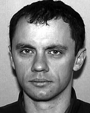 Bartek Pawlak合作论文数7W Wytze Keuning合作论文数7P.J. Gellings合作论文数7
 Noemi Leick合作论文数7J MEDEMA合作论文数6G. Mannino合作论文数6Rob Wolters合作论文数6f c van den heuvel合作论文数6e c e van grunsven合作论文数6K. van der Tak合作论文数6j c hooker合作论文数6Jan Verhoeven合作论文数6Eric van den Heuvel合作论文数6
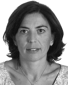 Lourdes Pelaz合作论文数E.T.S.I. de Telecomunicación, Universidad de Valladolid6
 Baggetto Loïc合作论文数Div Mat Sci & Technol, Oak Ridge Natl Lab6Pierre Woerlee合作论文数6




