Anyone who has spent any time with Mark knows that he loves puzzles. His office at Stanford is full of puzzles: some he built himself, some crafted from beautiful hardwood, and some simple children's toys. Each of them has their own aesthetic and their unique attraction to Mark. So, in many ways, it's no surprise that what attracted him to cofounding Rambus back in 1990 was a puzzle posed by Rambus cofounder Mike Farmwald: could they, using circuit and architecture techniques, increase the bandwidth of the dynamic random access memory (DRAM) interface tenfold without changing process technology?
A 40 Gb/s serial link interface is presented that includes four lanes of transceiver optimized for chip-to-chip communication while compensating for 20 dB of channel loss. Transmit equalization consists of a 2-tap feed-forward equalizer (FFE) while receive equalization includes a 2-tap FFE using a transversal filter, a 3-stage continuous-time linear equalizer with active feedback, and discrete-time equalizers consisting of a 17-tap decision feedback equalizer (DFE) and a 3-tap sampled FFE. The receiver uses quarter-rate double integrate-and-hold sampling. The clock and data recovery (CDR) unit uses a split-path CDR/DFE design which facilitates wider bandwidth and lower jitter simultaneously. A phase detection scheme that filters out edges affected by residual inter-symbol interference allows recovering a low-jitter clock from a partially-equalized eye. A fractional-N PLL is implemented for frequency offset tracking. Combining these techniques, the digital CDR recovers a stable 10 GHz clock from an eye containing 0.8 UIp-p input jitter and achieves 1-10 MHz of tracking bandwidth. The transceiver achieves horizontal and vertical eye openings of 0.27 UI and 120 mV, respectively, at BER = 10(-9). The quad SerDes is realized in 28 nm CMOS technology. Amortizing common blocks, it occupies 0.81 mm(2) per lane and achieves 23.2 mW/Gb/s power efficiency at 40 Gb/s.
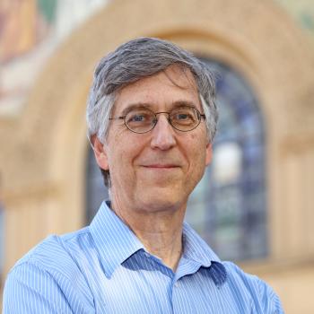 Mark Horowitz合作论文数Department of Electrical Engineering, Stanford University;Department of Computer Science, School of Engineering, Stanford University45
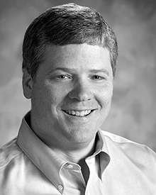 Kevin S Donnelly合作论文数41
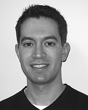 Brian Leibowitz合作论文数31
 Vladimir Stojanovic合作论文数Berkeley Wireless Research Center, University of California, Berkeley;Center for Energy Efficient Electronics Science, University of California, Berkeley;Berkeley Emerging Technologies Research Center, University of California, Berkeley22
 Carl W. Werner合作论文数University of California;Rambus Inc;University of California , Berkeley|Rambus Inc21
 Alfredo Moncayo合作论文数19Craig Hampel合作论文数19
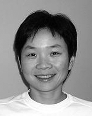 Jihong Ren合作论文数Jihong presents her farewell intern talk to SunLabs audience,
Contact About Sun News Employment Privacy Terms of Use Trademarks Copyright 1994-2007 Sun Microsystems, Inc19richard m barth合作论文数17
Jihong Ren合作论文数Jihong presents her farewell intern talk to SunLabs audience,
Contact About Sun News Employment Privacy Terms of Use Trademarks Copyright 1994-2007 Sun Microsystems, Inc19richard m barth合作论文数17 Bruno W. Garlepp合作论文数17
 Haechang Lee合作论文数14
 Stefanos Sidiropoulos合作论文数Center for Integrated Systems;Stanford University;Center for Integrated Systems, Stanford University14Jun Kim合作论文数13
 Fred Chen合作论文数13
 william stonecypher合作论文数12
 Pak Shing Chau合作论文数12
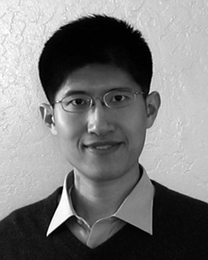 qi lin合作论文数11
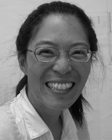 grace tsang合作论文数10
 Barry Daly合作论文数10
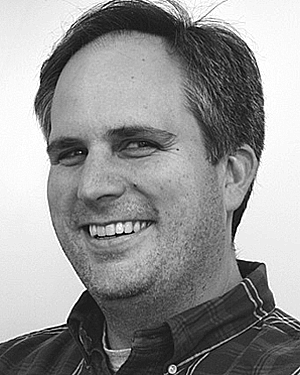 John C. Eble合作论文数10
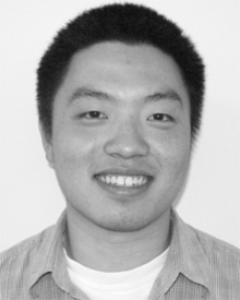 Andrew Ho合作论文数10Masum Hossain合作论文数9donald c stark合作论文数8
 Carsten Werner合作论文数Department of Chemistry and Food Chemistry, Technische Universität Dresden/Center for Regenerative Therapies Dresden, Technische Universität Dresden7frederick a ware合作论文数6teva j stone合作论文数6scott best合作论文数6
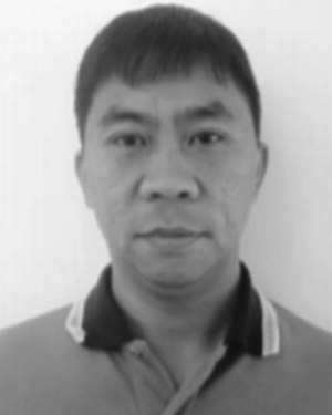 Yohan Frans合作论文数6Kollipara, R.合作论文数6
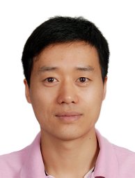 Lei Luo合作论文数Research Center for Eco-Environmental Sciences, Chinese Academy of Sciences6
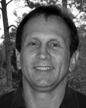 Wayne D. Dettloff合作论文数6leung yu合作论文数5benedict c lau合作论文数5tsyrchyang ho合作论文数5
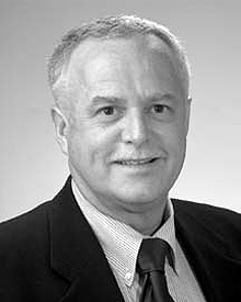 Thrush, T.P.合作论文数5
 roxanne vu合作论文数5
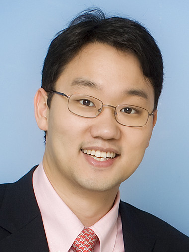 Jaeha Kim合作论文数Scientific Analog, Inc.;Department of Electrical and Computer Engineering, Seoul National University5
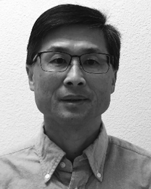 Simon Li合作论文数5
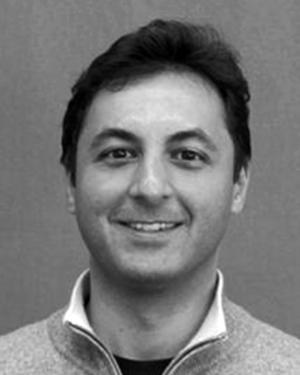 Kambiz Kaviani合作论文数5
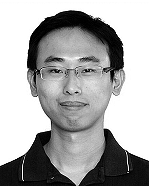 E.-Hung Chen合作论文数5B Garlepp合作论文数4Chau, P.S.合作论文数4billy w garrett合作论文数4t h lee合作论文数4j m wilson合作论文数4
 Nhat Nguyen合作论文数4Garlepp, B.W.合作论文数4
 Elad Alon合作论文数Department of Electrical Engineering and Computer Sciences, University of California, Berkeley;Berkeley Wireless Research Center, University of California, Berkeley4Clemenz Portmann合作论文数4




