The development of semiconductors is always accompanied by the progress in controllable doping techniques. Taking AlGaN-based ultraviolet (UV) emitters as an example, despite a peak wall-plug efficiency of 15.3% at the wavelength of 275 nm, there is still a huge gap in comparison with GaN-based visible light-emitting diodes (LEDs), mainly attributed to the inefficient doping of AlGaN with increase of the Al composition. First, p-doping of Al-rich AlGaN is a long-standing challenge and the low hole concentration seriously restricts the carrier injection efficiency. Although p-GaN cladding layers are widely adopted as a compromise, the high injection barrier of holes as well as the inevitable loss of light extraction cannot be neglected. While in terms of n-doping the main issue is the degradation of the electrical property when the Al composition exceeds 80%, resulting in a low electrical efficiency in sub-250 nm UV-LEDs. This review summarizes the recent advances and outlines the major challenges in the efficient doping of Al-rich AlGaN, meanwhile the corresponding approaches pursued to overcome the doping issues are discussed in detail.
Abstract AlGaN‐based ultraviolet light‐emitting diodes (UV‐LEDs) have the advantages of mercury (Hg) pollution free, small size, high efficiency, and so on, and are widely used in military, medical, and industrial fields, which are considered to be the most promising alternative to the traditional Hg lamps. Great efforts are made over the past few decades to improve the device performance, thereby meeting the commercial production and application requirements of UV‐LEDs, which is always accompanied by a series of interesting physical topics. In this review, the recent research progress in performance of AlGaN‐based UV‐LEDs is summarized from the perspectives of electrical injection, electro‐optical conversion, and light extraction, which are responsible for the operation of devices. The detailed discussions include the major challenges, the corresponding technological breakthroughs, and also the outlook of material growth, energy band modulation, as well as device fabrication involved in UV‐LEDs, which are expected to be helpful for the thorough comprehension of device physics and further development of AlGaN‐based UV‐LEDs.
The formation of spiral hillocks during AlGaN growth is investigated by modulating the residual strain in the underlying AlN templates. It is demonstrated that the high-density hillocks are directly related to the compressive stress, in particular for AlGaN on high-temperature annealed (HTA) AlN. AlN/AlGaN stress modulation multilayer is then introduced and optimized before AlGaN growth, which is revealed to be helpful to release the compressive stress in AlGaN as well as to suppress the hillocks. Eventually, the hillocks in AlGaN/HTA-AlN are eliminated, leading to a great improvement of yield for deep-ultraviolet light-emitting diode (DUV-LED) wafers. This work will definitely promote further industrial development and application of DUV-LEDs.
Enhancing the conductivity in Al-rich n-AlGaN is a key issue for realizing AlGaN-based ultraviolet light-emitting diodes (UV-LEDs) with low operating voltage and high wall-plug efficiency, especially in a planar geometry of flip–chip configuration. An approach of modulation doping is herein proposed, where an alternating-layer structure consisting of Si-doped and unintentionally doped AlGaN is assembled to achieve the spatial separation of electron activation and transport. As massive electrons diffuse from the AlGaN:Si layer into the neighboring i-AlGaN ones and then drift, the ionized-donor scattering is effectively weakened, leading to a significant enhancement of mobility as well as conductivity. An impressive electrical property of n-Al0.6Ga0.4N with a lateral conductivity of 201.7 S/cm is realized as a consequence, being 2.1 times of that in the continuously doped one. Furthermore, the operating voltage of 280 nm UV-LEDs is correspondingly reduced by 0.1–0.2 V at 100 mA by adopting modulation-doped n-AlGaN in the n-cladding layer.
A ground-breaking roadmap of III-nitride solid-state deep-ultraviolet light emitters is demonstrated to realize the wafer-scale fabrication of devices in vertical injection configuration, from 2 to 4 inches. The epitaxial device structure is stacked on a GaN template instead of conventionally adopted AlN, where the primary concern of the tensile strain for Al-rich AlGaN on GaN is addressed via an innovative decoupling strategy, making the device structure decoupled from the underlying GaN template. Moreover, the strategy provides a protection cushion against the stress mutation during the removal of substrates. As such, large-sized wafers can be obtained without surface cracks, even after the removal of the sapphire substrates by laser lift-off. Wafer-scale fabrication of 280 nm vertical injection deep-ultraviolet light-emitting diodes is eventually demonstrated, where a light output power of 65.2 mW is achieved at a current of 200 mA, largely thanks to the significant improvement of light extraction. This work will definitely speed up the application of III-nitride solid-state deep-ultraviolet light emitters featuring high performance and scalability. The efficiency of deep-ultraviolet light sources is critical for applications like disinfection. Here, the authors employ a novel decoupling strategy using GaN templates to fabricate 280 nm vertical injection diodes, achieving a light output power of 65.2 mW at 200 mA.
We attempt to improve the light extraction of AlGaN-based deep-ultraviolet light-emitting diodes (DUV-LEDs) by introducing a highly transparent p-type layer together with reflective Rh/Al p-type electrodes. The p-GaN contact layer is thinned to balance the Ohmic contact and DUV light transmittance, which helps the Rh/Al p-type electrodes realize high reflection as well as good electrical performance. After optimization, the Rh/Al reflective p-type electrodes present reflectance of greater than 70% and specific contact resistivity of 3.75 × 10⁻⁴ Ω·cm2. Due to the improvement in the light extraction efficiency, the highest wall-plug efficiency of 278 nm DUV-LEDs is improved by 57% compared to the conventional configuration with Ni/Au as the p-type electrodes.
Improving light extraction efficiency (LEE) of AlGaN-based deep-ultraviolet (DUV) light emitting diodes (LEDs) has been attempted by thinning the p-AlGaN/p-GaN layer and adopting Ni/Au/Al composite electrodes. It is found that the thin p-AlGaN/p-GaN layer can reduce the light absorption and the Ni/Au/Al electrodes achieve high reflectivity and Ohmic contact to ensure the enhancement of the light extraction and maintain fine electrical properties. By this approach, the maximum external quantum efficiency of the DUV-LEDs with optimized Ni/Au/Al reflective electrodes is increased by 40%, compared to that with conventional Ni/Au electrodes over the whole current range.
Solving the doping asymmetry issue in wide-gap semiconductors is a key difficulty and long-standing challenge for device applications. Here, a desorption-tailoring strategy is proposed to juggle the carrier concentration and transport. Specific to the p-doping issue in Al-rich AlGaN, self-assembled p-AlGaN superlattices with an average Al composition of over 50% are prepared by adopting this approach. The hole concentration as high as 8.1 × 1018 cm-3 is thus realized at room temperature, which is attributed to the significant reduction of effective Mg activation energy to 17.5 meV through modulating the activating path, as well as the highlighted Mg surface-incorporation by an intentional interruption for desorption. More importantly, benefiting from the constant ultrathin barrier thickness of only three monolayers via this approach, vertical miniband transport of holes is verified in the p-AlGaN superlattices, greatly satisfying the demand of hole injection in device application. 280 nm deep-ultraviolet light-emitting diodes are then fabricated as a demo with the desorption-tailored Al-rich p-AlGaN superlattices, which exhibit a great improvement of the carrier injection efficiency and light extraction efficiency, thus leading to a 55.7% increase of the light output power. This study provides a solution for p-type doping of Al-rich AlGaN, and also sheds light on solving the doping asymmetry issue in general for wide-gap semiconductors.
Surface kinetics in Al-rich AlGaN growth are regulated to realize a growth window allowing a higher rate as well as a lower temperature. Hence a rate of 2.3 μm h−1 at 1050 °C is achieved for n-Al0.55Ga0.45N with the typical step-terrace morphology.
Correlation between electrical properties and growth dynamics for Si-doped AlGaN with Al mole fraction above 60% has been investigated. It is found that the electron concentration decreases significantly when decreasing the growth rate, while the electron mobility experiences a non-monotonic process of increasing at first and then decreasing. Combination of secondary ion mass spectroscopy and panchromatic cathodoluminescence results, reveals that the evolution of electrical properties mainly originates from compensation of III vacancy (V-III) to Si dopant, making V-III-nSi complexes, i.e., the concentrations of V-III-nSi complexes increase with decreasing the growth rate, implying high growth rate principle is vital for n-AlGaN.
Efficient reduction of dislocations is a key topic in heteroepitaxial AlN films for optoelectronic or electronic applications. For this purpose, we explore a strategy of supersaturated vacancy engineering to promote the climb and meeting of dislocations. Through the intentional incorporation and subsequent thermal desorption of heteroatoms, the thermodynamic limitation for vacancy concentration under equilibrium conditions is broken, i.e., the concentration depends directly on the desorption number of heteroatoms, instead of formation energy. As such, extrinsic supersaturated vacancies can be introduced, significantly magnifying the climb of dislocations and thus enhancing the probability of dislocation meeting and annihilating. Specifically, the supersaturated vacancy engineering is applied to AlN on sapphire with a lattice mismatch as high as 13.3%, which demonstrates a threading dislocation density of 1.56 × 108 cm−2, one order of magnitude lower than that by conventional methods. Furthermore, 280-nm deep-ultraviolet light-emitting diodes are fabricated on such AlN template, and the light output power reaches 39.1 mW at 200 mA, 56% better than that without this approach. This study sheds light on the effective control of vacancies and dislocations and then paves the way for heteroepitaxial films of high quality, as well as consequent optoelectronic or electronic devices of high performance.
Growth of AlGaN-based multiple quantum wells (MQWs) with an IQE > 80% at room temperature has been realized on nano-patterned sapphire substrates. A DUV-LED device is then fabricated taking such high IQE MQWs as the active region.
High-quality AlN with uniform in-plane strain has been attempted with preset strain modulation on nano-patterned AlN templates (NPATs). It is found that this strain preset frame can effectively improve both the tilt and twist features of AlN on NPATs, further greatly decreasing threading dislocation density. More importantly, the AlN epilayer after completing coalescence can maintain the in-plane uniform compressive strain. Adopting AlN templates achieved in this scheme, the chip-on-wafer light output power (LOP) of AlGaN light-emitting diode (LED) reaches 10.2 mW at 100 mA with single emission peak at 280 nm, which increases by 22.3% than the LOP of LED device without adopting this strain preset frame.
Hall data for a p-Al0.4Ga0.6N/Al0.67Ga0.33N superlattice layer. The hole concentration in this p-AlGaN superlattice layer is 3.7×1018 cm-3 at room temperature.
The stress evolution behavior of AlN grown on nano-patterned substrates (NPSSs) has been investigated. It is found that there are two sources of the tensile stress for AlN grown on NPSSs. One originates from the coalescence of grain islands of the AlN nucleation layer, and then the voids provide a channel for the gradual release of the tensile stress to nearly stress-free state accompanied by the lateral growth process of the AlN columns on the mesas. The other originates from the contacting of adjacent columns to complete the coalescence process, which is responsible for the residual tensile stress in the top AlN epilayer after completing the coalescence. This understanding of the stress evolution is certainly of great significance in AlN-based material and devices.
A comprehensive strategy of crystal quality control for AlN grown on a nano-patterned sapphire substrate has been explored based on the period size effect. It is found that the crystalline perfection of AlN can be greatly improved by enlarging the period size from 1.0 to 1.4 μm, and the X-ray diffraction ω-scan FWHM values for (0002) and (10-12) planes reach 162 and 181 arcsec, respectively, owning to the significantly reduced area ratio of the coalescence zone. Our results indicate the pattern design requires a critical balance between reducing the area ratio of the coalescence zone and decreasing the coalescence thickness.
Influence of sapphire pretreatment conditions on crystalline quality of AlN epilayers has been investigated by metal organic chemical vapor deposition (MOCVD). Compared to alumination treatment, it is found that appropriate sapphire nitridation significantly straightens the surface atomic terraces and decreases the X-ray diffraction (0002) full width at half maximum (FWHM) to a minimum of 55 arcsec, indicating a great improvement of the tilting feature of the grain structures in the AlN epilayer. More importantly, there is no inversion domains (IDs) found in the AlN epilayers, which clarifies that optimal sapphire nitridation is promising in the growth of high quality AlN. It is deduced that the different interfacial atomic structures caused by various pretreatment conditions influence the orientation of the AlN nucleation layer grains, which eventually determines the tilting features of the AlN epilayers.
We report epitaxial growth of AlN films with atomically flat surface on nano-patterned sapphire substrates (NPSS) prepared by nano-imprint lithography. The crystalline quality can be greatly improved by using the optimized 1-μm-period NPSS. The X-ray diffraction ω-scan full width at half maximum values for (0002) and (102) reflections are 171 and 205 arcsec, respectively. The optimized NPSS contribute to eliminating almost entirely the threading dislocations (TDs) originating from the AlN/sapphire interface via bending the dislocations by image force from the void sidewalls before coalescence. In addition, reducing the misorientations of the adjacent regions during coalescence adopting the low lateral growth rate is also essential for decreasing TDs in the upper AlN epilayer.
Two AlGaN samples with different strain were designed to investigate mechanism of stress-driven composition evolution. It is discovered that AlGaN grown on AlN or (AlN/GaN superlattices (SLs))/GaN both consist of two distinct regions with different compositions: transition region and uniform region, which is attributed to the compositional pulling effect. The formation of the transition region is due to the partial stress release caused by the generation of misfit dislocations near the hetero-interface. And the Al composition in the uniform region depends on the magnitude of residual strain. The difference in relaxation degree is 80.5% for the AlGaN epilayers grown on different underlayers, leading to a large Al composition difference of 22%. The evolutionary process of Al composition along [0001] direction was investigated in detail.
By employing a single AlGaN layer with low Al composition, high quality and uniformity AlGaN/GaN heterostructures have been successfully grown on Si substrates by metal-organic chemical vapor deposition (MOCVD). The heterostructures exhibit a high electron mobility of 2150 cm2/Vs with an electron density of 9.3 × 1012 cm−2. The sheet resistance is 313 ± 4 Ω/◻ with ±1.3% variation. The high uniformity is attributed to the reduced wafer bow resulting from the balance of the compressive stress induced and consumed during the growth and the thermal tensile stress induced during the cooling down process. By a combination of theoretical calculations and in situ wafer curvature measurements, we find that the compressive stress consumed by the dislocation relaxation (~1.2 GPa) is comparable to the value of the thermal tensile stress (~1.4 GPa) and we should pay more attention to it during growth of GaN on Si substrates. Our results demonstrate a promising approach to simplifying the growth processes of GaN-on-Si to reduce the wafer bow and lower the cost while maintaining high material quality.
 Xinqiang Wang (王新强)合作论文数Institute of Condensed Matter and Material Physics, School of Physics, Peking University22
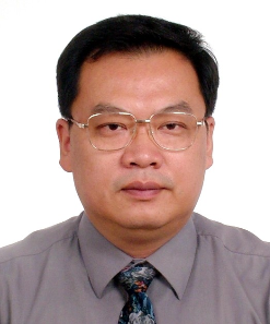 Bo Shen (沈波)合作论文数School of Physics, Peking University22
 Fujun Xu (许福军)合作论文数School of Physics, Peking University22
 Weikun Ge (葛惟昆)合作论文数Xinya College, Tsinghua University;Department of Physics, Tsinghua University19
 Jing Lang合作论文数16
 Xuelin Yang (杨学林)合作论文数Institule of Condensed Matter and Material Physics, School of Physics, Peking University16
 Xiangning Kang (康香宁)合作论文数Institute of Condensed Matter and Material Physics, School of Physics, Peking University15
 Zhixin Qin (秦志新)合作论文数School of Physics,Peking University13Xuzhou Fang (方绪周)合作论文数11Zhang Lisheng合作论文数11
 Ning Tang (唐宁)合作论文数School of Physics, Peking University9Baiyin Liu合作论文数7Xueqi Guo合作论文数7Chen Ji合作论文数7
 Zhizhong Chen (陈志忠)合作论文数Institute of Condensed Matter and Material Physics, School of Physics, Peking University7Liubing Wang合作论文数6Na Zhang合作论文数5Ziyao Zhang合作论文数5
 Chenguang He合作论文数4Fuyun Tan合作论文数3Mingxing Wang合作论文数3Yuanhao Sun合作论文数3Nan Xie合作论文数3Zhang Xia (张霞)合作论文数2Yong Wu合作论文数2Weiying Wang合作论文数2
 Peng Jin (金鹏)合作论文数Institute of Semiconductors, Chinese Academy of Sciences;University of Chinese Academy of Sciences2
 Lin Lu (鲁麟)合作论文数安徽工程大学电气工程学院2
 Wei Li合作论文数Department of Biological Chemistry, School of Medicine, University of California, Irvine;Division of Computational Biomedicine, School of Medicine, University of California, Irvine;Dan L. Duncan Cancer Center, University of California, Irvine2
 Zhijian Yang (杨志坚)合作论文数北京大学物理学院凝聚态物理与材料物理研究所2Wei An合作论文数1
 Yan Wang合作论文数1
 Bowen Sheng (盛博文)合作论文数School of Integrated Circuits, Peking University1ChengCheng Huang合作论文数1zhengyu xu合作论文数1Lei Guo合作论文数1Jianpeng Cheng合作论文数1
 Lisheng Zhang (张礼生)合作论文数Institute of Plant Protection, Chinese Academy of Agricultural Sciences;Shanghai Veterinary Research Institute, Chinese Academy of Agricultural Sciences1
 Jie Zhang (张洁)合作论文数College of Chemistry and Molecular Engineering, Peking University1
 Ji Chen (陈基)合作论文数Department of Physics, Peking University1Hou Mengjun合作论文数1Weiwei Guo合作论文数1
 Xinzheng Li (李新征)合作论文数School of Physics, Peking University1
 Shan Zhang合作论文数Peking University, Peking University1Ling Sang合作论文数1
 Jie Song (宋杰)合作论文数College of Software Technology, Zhejiang University;College of Computer Science and Technology, Zhejiang University1
 Jing Lv (吕劲)合作论文数Institute of Condensed Matter Physics and Material Physics, School of Physics, Peking University1
 Yonghai Chen (陈涌海)合作论文数Institute of Semiconductors, Chinese Academy of Sciences1
 Maojun Wang (王茂俊)合作论文数School of Integrated Circuits, Peking University1




