Recently, a laser-scanning technique for patterning Si-induced layer disordering of GaAs-AlGaAs heterostructures has been reported. This process, called laserassisted disordering (LAD), has been successfully used to fabricate low threshold buried heterostructure lasers. In this report, the LAD process is studied in detail with scanning electron microscopy, transmission electron microscopy and secondary ion mass spectrometry. The results are discussed in the context of device fabrication.
We discuss the advantages of quantum well solar cells (QWSCs) for thermophotovoltaic (TPV) applications and illustrate them with InP/InGaAs and GaInAsP/InGaAs QWSCs which were designed for other applications and have not been optimised for TPV. It is shown that an InP p-i-n solar cell with 15 lattice matched InGaAs quantum wells (QWs) in the i region has an increase in open circuit voltage ( V oc ) of (1.7 ± 0.1) times that of a control cell of InP with InGaAs in the i-region under an illuminating spectrum close to that expected from an ideal ytterbia emitter. Also, using an InGaAsP quaternary cell of band gap wavelength of 1.1 Am with 60 InGaAs QWs under the same illuminating spectrum the current density is increased by a factor of (2.4 ± 0.1) over that of the InP QWSC. The quaternary cell also absorbs longer wavelengths without any significant loss in V OC . Better temperature coefficients for the former quantum well solar cell than the control cell are observed in a spectrum approximating a black body at 3000 K. Further advantages of QWs for narrow band and broad band illuminating spectra are discussed.
Carrier escape from InP/AlGaAs single quantum well structures is studied by means of simultaneous steady state photocurrent and photoluminescence measurements. The activation energy for escape is measured for the first time in this system. The photoluminescence from the InGaAs wells indicates that a significant number of carriers do not escape at room temperature thus affecting the temperature dependence of the cell. An estimate of the nonradiative efficiency of the device studied is given as a function of bias and temperature. The relevance to new applications is discussed.
Two approaches have been used to fabricate stable photoelastic waveguides with planarized surfaces on GaAs-AlGaAs heterostructures. The first approach uses tensile Ni3GaAs stressors formed by metal-semiconductor reactions, The second approach uses inert, refractory and compressive stressors, such as RF sputtered W and RF co-sputtered WNi films, For comparison purposes, ridge waveguides have also been fabricated using the same heterostructure by a dry etching technique, Optical losses of photoelastic waveguides, measured by Fabry-Perot (FP) method at a wavelength of 1.53 mu m, are comparable to or better than those of the ridge waveguides, Material loss appears to be the primary loss mechanism in both photoelastic and ridge waveguides, These results indicate that the photoelastic waveguide processing technique reported in this study is a promising alternative to commonly used dry etching techniques for planarization.
The mode behavior of symmetric air-post vertical cavity surface emitting lasers is investigated using a unique tandem triple-pass Fabry–Perot interferometer as well as standard characterization techniques. A series of high resolution spectra taken at various current levels demonstrates relaxation oscillations of the fundamental mode and the lifting of mode degeneracy by crystal birefringence and structural anisotropy. Near field images and L–I measurements identify the discontinuous jumps in mode number and polarization.
The design, fabrication, and characterization of monolithically integrated single- and dual-stage cascadable optical differential amplifiers (ODA's) are presented, The circuits are realized with photodiodes (PD's), metal-semiconductor field-effect transistors (MESFET's) and light-emitting diodes (LED's) in the GaAs-AlGaAs system. They are fabricated with a process which uses trench technology for the separation of the devices. The single-stage switching energy of 2.5 pJ is reduced to 0.4 pJ by the addition of a second stage, thereby increasing the bandwidth from 2 to 12 MHz. The output power is 30 mu W, and the measured contrast ratio is approximately 1000, Switching is possible over an input power range of more than 5 decades, with a lower limit of 15 pW. We measure an optical open-loop gain of 2.10(6) and a power dissipation of 15-20 mW.
The authors report on lattice matched InP/InxGa1-x As multiple quantum well solar cells (QWSCs). An alternative method of p-doping is used, which allows the dopant to diffuse from a highly doped InGaAs cap into an underlying InP layer which has no deliberate doping. They discuss an important experimental technique, the measurement of the monochromatic photocurrent as a function of bias, used to test this approach to p-doping of InP. A model has been developed and theoretical fits of the spectral response (SR) of several multiple quantum well (MQW) samples are shown. They present results that show the enhancement of the short-circuit current (ISC) over a comparable InP cell and the enhancement of the open-circuit voltage (V OC) over an InP/InGaAs double heterostructure. This is the first observation of QWSC efficiency enhancement over comparable conventional solar cells made from the well material alone
A ridge waveguide GaAs/AlGaAs DBR laser with a nonabsorbing grating section and a monolithically integrated transparent waveguide has been fabricated by the use of vacancy-enhanced quantum well disordering (VED). This technique allows the definition of absorbing and transparent regions, and requires only a single growth step. No VED-enhanced degradation of the laser quality was noted. The optical output power was 5 mW from both the cleaved facet and the grating reflector, threshold currents were 25 mA and the slope efficiencies were 0.2 W/A.
Wavelength-shifted GaAs/AlGaAs Fabry–Pérot ridge waveguide lasers were fabricated by vacancy-enhanced quantum well disordering using dielectric cap annealing. 500 μm long and 4 μm wide Fabry–Pérot lasers with emission wavelengths selectively shifted by 20 nm were integrated with unshifted lasers on the same chip, characterized and further compared with lasers fabricated from as-grown material. These investigations showed that the absorption edge of a single-quantum well double heterostructure can be selectively blueshifted after epitaxial growth without compromising diode laser performance.
The evolution of surface topography during epitaxial growth of AlxGa1-xAs (0 less than or equal to x less than or equal to 1) is observed using angle-resolved elastic light scattering within a metalorganic vapor phase epitaxy system. The density and orientation of extended topographical features are monitored during various growth phases: annealing, initiation, steady state, and conclusion. Transient monolayer oscillations and persistent fluctuations in surface roughness are observed. Also shown are the emergence of [0(1) over bar1$] oriented B-steps and the dependence of the topography upon V/III ratio.
The monolithic integration of a GaAs-AlGaAs distributed Bragg reflector (DBR) laser with a nonabsorbing grating section, a transparent waveguide, and an absorbing photodetector is reported. Transparent and absorbing segments were defined after growth by vacancy-enhanced quantum-well disordering (VED). Laser output power was 5 mW with a threshold current of 22 mA. Detector current was linearly dependent on the laser output power and the emission from the grating side of the laser could be directly coupled into the detector. The conversion efficiency, defined as the ratio between detector current and laser output power, was 0.47 A/W. Using a comparison with as-grown, SiO/sub 2/-capped and SrF/sub 2/-capped devices, both lasers and detectors were not seen to be adversely affected by the anneal required for the VED.<>
The surface topography during initial and steady state epitaxial growth of InP on InP is monitored with in situ diffuse elastic light scattering. The in situ results are compared with the end-of-run topography measured by ex situ atomic force microscopy. Upon growth initiation, an increase in surface roughness is observed with steps oriented perpendicular to the [011] and [010] direction. After several nanometers of InP deposition, the surface topography planarizes and steady state step-flow epitaxy develops with steps aligned to the pregrowth terrace.
A ridge waveguide GaAs/AlGaAs quantum well DBR laser fabricated with a simplified grating recess-technology and a third order prating is described. The reflector is fabricated on top of a recessed waveguide using holographic exposure followed by reactive ion etching. The laser operates on a single longitudinal and lateral mode with threshold current as low as 20mA, output power 5mW per facet and is intended for monolithically integrated interferometer applications.
The evolution of surface topography during epitaxial growth of lattice matched InP/InGaAs/InP on (100) InP substrate is observed using in situ elastic light scattering supported by ex situ atomic force microscopy. A topographically smooth growth transition from InP to InGaAs is observed. However, the InP-on-InGaAs interface exhibits three-dimensional nucleation followed by planarization and two-dimensional epitaxy. The three-dimensional phase is a result of the high surface energy of InP relative to InGaAs. A growth pause after the InGaAs QW increases the transient roughness of the InP surface and increases the thickness of InP required for planarization.
Aluminum-oxide thermally grown into high Al-concentration AlxGa1-xAs layers has recently been studied extensively. The material shows electrical and optical properties that make it useful in a semiconductor laser fabrication process where it can provide electrical isolation and optical guiding, as well as simplify the fabrication and integration process considerably. We use this thermal oxide to produce GaAs/AlGaAs semiconductor lasers that can be integrated with other devices. The GaAs cap- layer is masked with photoresist and the exposed GaAs areas are etched away, leaving a GaAs oxidation mask on the AlGaAs upper cladding layer. Using N2 carrier gas saturated with H2O vapor, the uncovered Al0.8Ga0.2As material is converted into a stable aluminum-oxide at temperatures around 450 degree(s)C. Due to the near-isotropic oxidation an `ellipsoidal' diffusion front is created, which is in strong contrast to the well-known mesa cross-section in conventional dry-etched ridge-waveguides but is more similar to e.g. wet-etched buried heterostruture lasers.
Magnetron dry etching using SiCl4, combined with a smooth reflowed photoresist masking technique has been used to fabricate GaAs/AlGaAs ridge waveguides. The effect of pressure, flowrate and power on etch rate and sidewall smoothness has been studied. Waveguides fabricated using optimum parameters exhibited optical losses lower than those achievable using wet etching. This process was further used in the fabrication of Fabry Perot ridge lasers, detectors and phase modulators.
The topographical evolution of the (100) GaAs surface annealed under an arsine/hydrogen ambient is studied by in situ orientation-resolved light scattering and ex situ atomic force microscopy (AFM). The light scattering system provides real-time monitoring of the magnitude and crystal orientation of topographical features of 0.3 μm scale. The AFM images of the GaAs surface, quenched at various annealing temperatures, vividly depict the randomly oriented high density monolayer steps evolving into an atomically smooth terracelike structure.
In situ elastic light scattering was used to characterize, in real-time, the topography of InP-InGaAsP and GaAs epitaxial layers grown by metalorganic chemical vapor deposition (MOCVD). Phenomena such as the evolution of the atomic terrace and interface included roughness were observed. Ex situ atomic force microscopy images provide corroboration of the in situ data
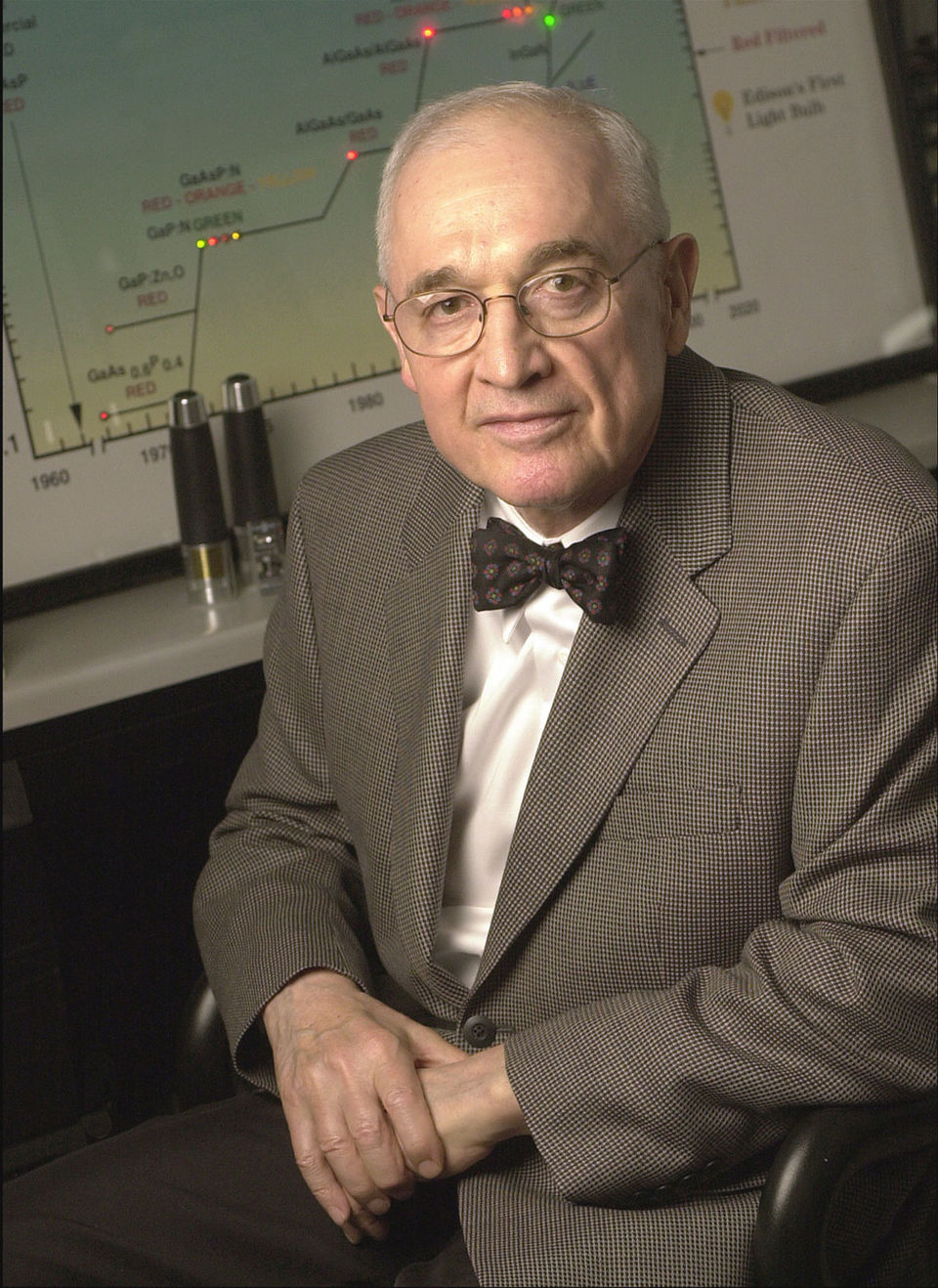 Nick Holonyak合作论文数Holonyak Micro & Nanotechnology Lab, The Grainger College of Engineering, University of Illinois at Urbana-Champaign42
 Burnham, R.D.合作论文数36Thomas L. Paol合作论文数Xerox Palo Alto Research Center34Robert L. Thornton合作论文数20thomas l paoli合作论文数16g s jackson合作论文数14
 Kuo-Cheng Hsieh合作论文数13R. Kaliski合作论文数10William Streifer合作论文数10
 Douglas C. Hall合作论文数9Chung, Harlan F.合作论文数9Hisashi Shichijo合作论文数9d g deppe合作论文数8Treat, D.W.合作论文数8
 Hans Zappe合作论文数Department of Microsystems Engineering, University of Freiburg7Derek W. Nam合作论文数7
 Richard Matyi合作论文数Dept . of Materials Sci . & Eng;Dept . of Materials Sci . & Eng .;University of Wisconsin-Madison;Dept . of Materials Sci . & Eng ., University of Wisconsin-Madison6W. E. Plano合作论文数6
 Louis Guido合作论文数Virginia Tech6Herbert P. Schweizer合作论文数5Hw Lehmann合作论文数4b graf合作论文数4H. G. Drickamer合作论文数4M. J. Peanasky合作论文数4
 Daniel Hofstetter合作论文数Neuchâtel Institute of Physics4c lindstrom合作论文数3Hans Sigg合作论文数Laboratory for Micro- and Nanotechnology, Paul Scherrer Institut3J. SöChtig合作论文数3
 Fernando Ponce合作论文数Department of Physics, Arizona State University3glen alan herrmannsfeldt合作论文数2alexander zachariou合作论文数2Ma Pate合作论文数2FJ ENDICOTT合作论文数2
 Peter Riel合作论文数2c h wu合作论文数2
 Kathleen Meehan合作论文数Bradley Dept. of Electr. & Comput. Eng., Virginia Tech;c;Bradley Dept. of Electr. & Comput. Eng., Virginia Tech2
 Paul Griffin合作论文数2Gavrilovic, P.合作论文数2John M Brown合作论文数2F. G. Kellert合作论文数2
 Jenny Nelson合作论文数Department of Physics, Faculty of Natural Sciences, Imperial College London2e s m tsui合作论文数1c lindstroem合作论文数1s gehrsitz合作论文数1m j ries合作论文数1Michael Camras合作论文数1j c tramontana合作论文数1m g craford合作论文数1Rd Bringans合作论文数1




