The interfacial interaction between Cr thin films and multi-component oxide glasses has been observed by means of high spatial resolution electron energy loss spectroscopy. Besides a partially oxidized Cr thin layer, a ~5nm wide Cr diffusion layer is seen. Chromium oxidation at the interface results from the difference between the heats of oxide formation. Ion exchange between Cr2+ and alkaline earth ions then causes the formation of the diffusion layer. The electronic states of the Cr in this diffusion layer are different from that in the oxidized layer. Strong interaction between Cr and O in the diffusion layer suggests that such a layer could be responsible for the formation of a strong Cr/glass interface.
Using a fifth-order aberration-corrected scanning transmission electron microscope, which provides a factor of 100 increase in signal over an uncorrected instrument, we demonstrated two-dimensional elemental and valence-sensitive imaging at atomic resolution by means of electron energy-loss spectroscopy, with acquisition times of well under a minute (for a 4096-pixel image). Applying this method to the study of a La0.7Sr0.3MnO3/SrTiO3 multilayer, we found an asymmetry between the chemical intermixing on the manganese-titanium and lanthanum-strontium sublattices. The measured changes in the titanium bonding as the local environment changed allowed us to distinguish chemical interdiffusion from imaging artifacts.
A study of the effects of small-angle specimen tilt on high-resolution annular dark field images was carried out for scanning transmission electron microscopes with uncorrected and aberration-corrected probes using multislice simulations. The results indicate that even in the cases of specimen tilts of the order of 1 degree a factor of 2 reduction in the contrast of the high-resolution image should be expected. The effect holds for different orientations of the crystal. Calculations also indicate that as the tilted specimen gets thicker the contrast reduction increases. Images simulated with a low-angle annular dark field detector show that tilt effects are more pronounced in this case and suggest that these low-angle detectors can be used to correct specimen tilt during scanning transmission electron microscopes operation.
A semiquantitative correlation between experimental observations and theoretical prediction in electron microscopy is achieved. Experiments conducted on amorphous silicon in the convergent beam electron diffraction mode provide measurements of the reduction of the central-disk intensity. In addition to elastic scattering the effects of multiple inelastic scattering of the probe electrons were incorporated into the theory describing beam propagation through the specimen. With incorporation of the dominant plasmon scattering a better than 10% match of the theory with experiment is observed indicating the critical role of multiple inelastic scattering in quantitative electron diffraction and imaging.
A study of high-resolution ADF imaging in uncorrected and aberration-corrected STEMs was carried out by multislice simulation. The presence of amorphous layers at the surface of a crystalline specimen is shown to significantly alter the visibility of the atomic columns. After propagating through an amorphous layer a portion of the beam passes without any alteration while scattered electrons introduce a Gaussian background. The dependence of the image contrast on the crystal structure, orientation and the types of the atoms present in the crystal was studied. In the case of uncorrected probes an amorphous layer thicker than 200 A is necessary to achieve considerable reduction of the visibility of the atomic columns, but with aberration-corrected probes only 60 A is necessary. With changes in defocus, crystalline specimens with amorphous layers on the top can also be imaged and high-resolution ADF images can be obtained. An amorphous layer at the beam entry surface affects the ADF image more than that of an amorphous layer at the exit surface. Approximately linear reduction of the contrast (with a slop of 1) is expected with increased thickness of amorphous layer.
Submitted for the MAR07 Meeting of The American Physical Society Spin Transfer Switching and Magnetization Dynamics in Py/Cu/Py Nanopillar Spin-Valves with Sidewall Oxide Passivation and Nonuniform Current Injection OZHAN OZATAY, KEE WEE TAN, PRAVEEN GOWTHAM, PATRICK M. BRAGANCA, ERIC MICHAEL RYAN, GREGORY D. FUCHS, JOHN C. READ, ANDRE K. MKHOYAN, MALCOLM G. THOMAS, KIRAN V. THADANI, JACK C. SANKEY, JOHN SILCOX, DANIEL C. RALPH, ROBERT A. BUHRMAN, Cornell University — The manipulation of magnetization, both to drive precessional dynamics and trigger magnetization reversal in nanomagnets by transferring spin angular momentum from a spin-polarized current, presents opportunities for better scalability in nanoscale magnetic memory devices and microwave oscillators. Some of the major practical concerns include reducing the current level needed to write magnetic bits in an error-free fashion at high operating speeds in memory devices as well as exciting highly coherent dynamic modes for nanoscale microwave oscillator applications. In this work we report on the detrimental effects of the adventitious antiferromagnetic oxides at the perimeter of Py/Cu/Py nanomagnets such as an anomalous increase in magnetic damping at low temperatures and stochastic fluctuations in switching fields. We find that in addition to sidewall oxide passivation, the concentrated spin torque from nonuniform injection also reduces the sidewall effects leading to a more efficient spin transfer switching mechanism as well as microwave dynamics. Ozhan Ozatay Cornell University Date submitted: 30 Nov 2006 Electronic form version 1.4
To identify major features in low electron energy loss spectra, the different excitations (bulk plasmons, interband transitions, surface plasmons, Cherenkov and surface guided modes) must be delineated from each other. In this paper, this process is achieved by noting the linear thickness dependence of bulk processes contrasted with the constant thickness behavior of surface excitations. An alternative approach of analyzing bulk plasmon-loss is also introduced. Using a new algorithm, the parameters of plasma generation-plasmon energy E(P,0), a damping parameter DeltaE(P) and the coefficient of the dispersion relation gamma were obtained from a single curve fitting on the example of Si. The ability to separate surface-losses from the rest of the data permitted identification of the fine structure of the surface-losses. The strong peak at 8.2 eV characteristic of non-radiative surface plasmon excitations was measured for Si. Analysis of surface excitations indicates that a 10ASiO2 surface coating layer is still present despite careful cleaning the specimen. Dielectric functions deduced from the EELS data prove to be considerably affected by the presence of the surface-losses for samples as thick as 800A.
Extended abstract of a paper presented at Microscopy and Microanalysis 2006 in Chicago, Illinois, USA, July 30 – August 3, 2006
A scanning transmission electron microscope (STEM) study of silicon–germanium alloying using annular dark field (ADF) or Z-contrast imaging and electron energy loss spectroscopy (EELS) is presented. Results and techniques are discussed. Growth of 11 equivalent monolayers of germanium on silicon at 650 °C results in dome-shaped islands or quantum dots that contain up to ∼40% silicon. The interface between the as-grown island and substrate shows a highly disordered or amorphous zone ∼1.5-nm wide directly under the island. Annealing for 60 min at 650 °C gives larger pyramidal islands with diffuse crystalline interfaces and an equilibrium distribution of up to ∼70% silicon in the islands.
An unusually complete recovery of extensive electron-beam-induced damage in a thin film of a CaO-Al2O3-SiO2 glass was discovered. Nanoscale measurements show that the Ca ions migrate about 10 nm away during irradiation and return during recovery. Oxygen atoms are trapped largely as molecular oxygen and do not migrate. Electron energy loss measurements demonstrate that the glass returns completely to the original compositional and structural state thus indicating that the glass is in a deep thermodynamic energy minimum.
Analysis of the electron energy loss spectra of core-level electronic transitions, O K- and Ca L2,3-edges, combined with composition-sensitive annular dark field imaging shows that under electron-beam irradiation portlandite can easily be transformed into calcium oxide. The low-loss region of the energy loss spectra measured before and after transformation also supports the observations. Two possible mechanisms of the electron beam-induced modification of the specimen, radiolysis and knock-on damage, are discussed, and it was found that radiolysis is likely to be the primary mechanism for this transformation of Ca(OH)2 into CaO, while some knock-on damage is also expected.
With current advances in sub-angstrom resolution scanning transmission electron microscopy (STEM), it is now possible to image directly local crystal structures of materials where dramatically different atoms are separated from each other at distances about or less than 1 angstrom. We achieved direct imaging of atomic columns of nitrogen in close proximity to columns of aluminum in wurtzite aluminum nitride by using annular dark field imaging in an aberration-corrected STEM. This ability allows direct determination of the local polarity in nanoscale crystals and crystal defects.
We have used scanning transmission electron microscopy and electron energy-loss spectroscopy techniques to study the nature of interfacial interactions in a Ta/CuOx stack that give rise to a smooth surface morphology, which can be utilized for seeding thin magnetic multilayer devices. Our measurements reveal that the interfacial smoothing is mainly due to the preferential reaction of Ta with O at the Ta/CuOx interface assisted by grain boundary diffusion of oxygen which thereby acts to smooth out the surface roughness created by the large crystalline grains of Cu.
GaN quantum wells in an AlN matrix are characterized using scanning transmission electron microscopy. The width of the quantum wells and sharpness of the interfaces are measured with composition sensitive annular dark field imaging and electron energy-loss spectroscopy. The effects of beam broadening inside the specimen are discussed and mechanisms to minimize it are suggested. The quantitatively measured intensity of the N K-edge versus position is compared with the propagating beam intensity obtained from multislice calculations. Possible effects of strain in the structure on its electronic states and energy-loss spectra are also discussed.
Calculations of the electronic energy levels and the distribution of the quasi-two-dimensional electron gas (Q2DEG) at the GaN/AlxGa1−xN interface that take into account the graded nature of the interface are presented in this article. Mapping of the interface using scanning transmission electron microscopy annular dark-field imaging, the changes in the N K-edge and the integrated intensity of the Al L2,3-edge revealed that the interface can be up to 20 Å wide. Self-consistent calculations in the local density approximation estimate the sensitivity of the Q2DEG formed at the interface to various parameters, including the width of the interface, the concentration of bound charge, ambient temperature, and the geometrical sizes of the structure.
The contrast due to a strain field at an amorphous silicon/crystalline silicon (a-Si/c-Si) interface relative to the bulk crystal is studied with a scanning transmission electron microscope equipped with a low angle annular dark field (LAADF) detector and a high angle ADF (HAADF) detector. Experimental observations suggest that strain contrast depends closely on sample thickness and collection angle. For a thin sample (<100 Å) strain contrast is negative in both the LAADF and HAADF images. For a thick sample (>150 Å) strain contrast is positive in the LAADF image and negative in the HAADF image. Theoretical calculations of the effect of a random strain field are carried out. First, a simple model based on atomic scattering with an extra Debye–Waller factor is employed. It predicts a positive strain contrast in the LAADF image and no contrast in the HAADF image. The simple model fails for the HAADF contrast because it does not consider the propagation process of the electron beam inside the sample. Therefore multislice simulations including propagation details are carried out. The multislice simulation results agree well with the experimental observations. A measure of the strain amplitude is attained by comparing the experimental data with multislice simulation results. Quantitative measurements of strain contrast are only possible if the sample thickness is known.
Composition sensitive annular dark field imaging and electron energy-loss spectroscopy were used to determine long-range uniformities of GaN quantum wells and the sharpness of their interfaces grown in AlN matrix by molecular beam epitaxy. Low magnification annular dark field images reveal waviness along the growth plane with a period of ∼50 nm and a height ∼20 nm in one sample and significant changes of the long-range uniformity in the other. Measurements of the changes in energy-loss spectra of the Al L2,3, Ga L2,3, and N K edge across quantum well indicate that the interfaces between the quantum wells and the barriers are in most cases almost atomically sharp.
The electronic structure of wurtzite InN has been investigated by electron energy loss spectroscopy (EELS). Spectra of the nitrogen K edge and the indium M4,5 edge have been measured and were compared with calculated partial, N 2p and In 5p conduction band density of states in InN. Excellent agreement on the relative positions of the characteristic peaks were obtained. From low-loss EELS the bulk plasmon energy at 15.5 eV, location of the In 4d deep valence states at about 16.3 eV below the conduction band maximum and strong interband transitions with 6.2 eV excitation energy are also found.
In this letter, an alternative approach to determine the polarity of GaN thin films based on the atomic location by channeling-enhanced microanalysis technique is described. Theoretical calculations provide a straightforward criterion for polarity determination that is a major advantage of this method. At the Bragg position, the thickness-averaged incident electron intensity, and hence, electron induced characteristic x-ray yield, is higher on the N plane than on the Ga if the g vector of the diffraction beam is parallel to the Ga–N bond direction, and vice versa. Experimental results support the theoretical predictions. The possible errors in the experiments are also discussed.
Journal Article Effects of Detector Black Level in ADF-STEM Imaging Get access Z Yu, Z Yu Physics Department, Cornell University, Ithaca, NY 14853 Search for other works by this author on: Oxford Academic Google Scholar P E Batson, P E Batson IBM Thomas J. Watson Research Center, Yorktown Heights, NY 10598 Search for other works by this author on: Oxford Academic Google Scholar J Silcox J Silcox School of Applied and Engineering Physics, Cornell University, Ithaca, NY 14853 Search for other works by this author on: Oxford Academic Google Scholar Microscopy and Microanalysis, Volume 8, Issue S02, 1 August 2002, Pages 472–473, https://doi.org/10.1017/S1431927602105307 Published: 01 August 2002
 David Anthony Muller合作论文数Kavli Institute at Cornell for Nanoscale Science;School of Applied and Engineering Physics, Cornell University19
 Robert Buhrman合作论文数School of Applied and Engineering Physics, College of Engineering, Cornell University17
 Andre Mkhoyan合作论文数Department of Chemical Engineering and Materials Science, College of Science and Engineering, University of Minnesota17
 Philip E. Batson合作论文数Department of Physics and Astronomy, School of Engineering, Rutgers, The State University of New Jersey/Department of Materials Science and Engineering, School of Engineering, Rutgers, The State University of New Jersey15
 Earl J. Kirkland合作论文数School of Applied and Engineering Physics, Cornell University11
 CH CHEN合作论文数10Dk Lathrop合作论文数9
 Stephen E. Russek合作论文数National Institute of Standards and Technology, US Department of Commerce9William J. Schaff合作论文数8Sl Sass合作论文数7Roy Benedek合作论文数Argonne National Laboratory7D. A. Shashkov合作论文数7Richard Vanfleet合作论文数6S. Subramanian合作论文数6
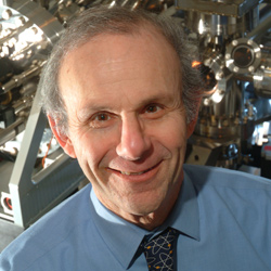 David Seidman合作论文数Department of Materials Science and Engineering, McCormick School of Engineering, Northwestern University;Center for Atom-Probe Tomography, Northwestern University6R. F. Loane合作论文数5Brian H. Moeckly合作论文数5J.L. Lee合作论文数4Lf Eastman合作论文数4S. Hillyard合作论文数4
 Lin Yang (杨霖)合作论文数School of Astronautics, Harbin Institute of Technology4E. S. Alldredge合作论文数4
 Richard D Leapman合作论文数Department of Health & Human Services, National Institute of Biomedical Imaging and Bioengineering4Zhiheng Yu (于志恒)合作论文数4TJ Eustis合作论文数4monica jean plisch合作论文数3R. Vincent合作论文数3
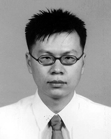 Chungho Lee合作论文数3Nan Jiang (姜楠)合作论文数3
 Hans Hallen合作论文数Department of Physics, College of Sciences, North Carolina State University3
 N W Ashcroft合作论文数Cornell University3Malcolm G. Thomas合作论文数3Tiao-Yuan Huang合作论文数3L. Pesenson合作论文数2
 Oleg I Lebedev合作论文数2D.P. Basile合作论文数2R H Wade合作论文数2Katine, J.A.合作论文数2Hj Gossmann合作论文数2hong wu合作论文数2
 Anne-Marie Haghiri-Gosnet合作论文数2Allen Jiang合作论文数Department of Physics, Arizona State University2
 B. Mercey合作论文数2
 Francis DiSalvo合作论文数Department of Chemistry & Chemical Biology, College of Arts & Sciences, Cornell University2
 Jianrong Qiu (邱建荣)合作论文数College of Optical Science and Engineering, Zhejiang University;State Key Laboratory of Modern Optical Instruments, Zhejiang University2
 G. Van Tendeloo合作论文数EMAT, University of Antwerp (RUCA), Groenenborgerlaan 171, B-2020 Antwerp, Belgium2L. A. Grunes合作论文数2
 R. Stanley Williams合作论文数Department of Electrical and Computer Engineering, College of Engineering, Texas A&M University2B. Moeckly合作论文数2




