This study evaluated the physical and mechanical properties of glass ionomer cement (GIC) associated with 5% hydroxyapatite nanoparticles (NPHAps) and 10% bioactive glass (BAG) 45S5 before and after brushing at different storage times. Surface roughness was evaluated using a rugosimeter, Vickers hardness using a microdurometer, and mass variation measured in an analytical balance at 1, 7, 15, 30, and 60 days before and after the brushing test, with the aid of toothbrushing simulator and soft bristle toothbrushes. Nonnormal distribution was observed, and the nonparametric Wilcoxon and Kruskal–Wallis tests followed by Dunn’s were performed, with a significance level of 5%. We observed higher values for mass loss on the first day for all groups. The surface roughness was lower in the control and NP groups, 30 days after brushing. Higher values for hardness were found in the control group and lower ones for NP, after brushing. The control and BAG groups presented a decrease in hardness over time. The NP group presented the highest values before brushing, while the control group had the highest values after brushing. The association of NPHPa with the GIC is the most promising combination, since it presented satisfactory values for surface hardness. However, conventional GIC not associated with NPHPa or BAG is still an option, since it is available in the market and the most economically viable option.
Polycrystalline Ca1-xSrxCu3Ti4O12 ceramics were studied as a function of the strontium content in order to understand its effects on the structure, microstructure and electrical characteristics of these compounds. Our results showed that the Sr2+ cationic substitution into the A sites of the initial CaCu3Ti4O12 (CCTO) phase leads to crystalline phases with specific stoichiometry. Although the same space group is observed, the cationic substitution induces larger lattice parameter, phase density, and chemical bonding length when compared to the initial CCTO phase. Microstructure results indicated that the strontium content has a significant influence on sample sinterability leading to changes in grain growth and densification process. The non-ohmic characterization showed that the Ca0.5Sr0.5Cu3Ti4O12 phase exhibits improved breakdown electric field (32 kV/cm), nonlinear coefficient (269) and lower leakage current (26 mu A), while the SrCu3Ti4O12 phase presents permittivity of about 5000 at 1 kHz.
The origin of abnormal ferroelectric and unusual piezoelectricity in the polycrystalline CaCu3Ti4O12 (CCTO) thin films deposited by RF-sputtering on Pt/Ti/SiO2/Si (100) substrates was explored. The CCTO thin films, deposited at room temperature followed by annealing at 600?C for 2 h in a conventional furnace, have a cubic structure with lattice parameter a = 7.379 ? 0.001 ? and without any secondary phases. No polarization loss up to 1010 switching cycles, with a switched polarization ?P of 30 ?C/cm2 measured at 400 kV/cm was evidenced. The piezoelectric coefficient investigated by piezoresponse force microscopy (PFM) was approximately 9.0 pm/V. This may be the very first example of exploring the origin of ferroelectric behaviour for a material that possesses space charge polarization with highly resistive grain boundaries in the polycrystalline state.
The need for faster, smaller, cheaper and energy-efficient electronic devices has been growing continuously in the last decade, with the conventional data storage technologies (i.e., static random access memory and dynamic random access memory), which have been so far fulfilled by CMOS-charge storage-based circuits, approaching their fundamental limits, due to the lesser progress of technology in comparison to logic. To overcome this challenge, increasingly high storage density memories has become one of the crucial approaches, aiming to improve storage capacity and reading/writing speed. A semiconductor memory is an indispensable component of all modern electronic devices, with all recognizable computing platforms, from hand-held devices to large supercomputer storage systems being used for storing data, temporarily or permanently. The ability of a material to store information is defined as a solid-state memory effect, which requires at least two switchable memory states that can be addressed by an externally controlled parameter. Based on storing data volatility, memories are basically classified into two categories, volatile and nonvolatile, with the former immediately losing the stored data after turning off the power, whereas the latter being capable of retaining the stored data for a longer period, even after the power is turned off. To optimize the performance-cost trade-off, hierarchical systems made from devices with varying speed, density, and cost have been adopted and the novel nonvolatile memory (NVM) concepts, such as ferroelectric random access memory, phase-change RAM, magnetic RAM, spin-transfer-torque RAM (STT-RAM), and resistive RAM (RRAM) are fulfilling the changing market trend requirements, from electronics to high performance computing, due to encouraging recent experimental demonstrations of high density, excellent scalability, low power consumption, endurance, and low cost. An RRAM is normally referred as those NVM technologies built on the resistance changing mechanisms, which can be varied by applying a voltage pulse, other than phase-change memory and STT-RAM. Data is stored by changing the resistance across a dielectric solid-state material in the RRAM cell, which presents two resistance states: a high-resistance state and a low-resistance state, being respectively defined as RON and ROFF. Thus, the device can be used as a Boolean logic switch returning (0) when the resistance is ROFF and (1) when RON.
In this work, a lanthanum (La) doped ceria (CeO2) film, which depicted a dual gas sensing response (electric and optical) for CO(g) detection, was obtained by the microwave-assisted hydrothermal (HAM) synthesis and deposited by the screen-printing technique, in order to prevent deaths by intoxication with this life-threatening gas. An electric response under CO(g) exposure was obtained, along with an extremely fast optical response for a temperature of 380 degrees C, associated with Ce+4 reduction and vacancy generation. A direct optical gap was found to be around 2.31 eV from UV-Vis results, which corresponds to a transition from valence band to 4f states. Due to the anomalous electron configuration of cerium atoms with 4f electrons in its reduced state, they are likely to present an electric conduction based on the small polaron theory with a hopping mechanism responsible for its dual sensing response with a complete reversible behaviour. (C) 2017 Elsevier B.V. All rights reserved.
Efeito da temperatura sobre a autoindução magnética do níquel e da platina e a permeabilidade magnética do níquel, no intervalo de temperatura de 525K a 620K, confirma dados encontrados na literatura.
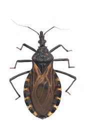
Trypanosoma cruzi, the etiological agent of Chagas disease, is transmitted by triatomines that have been described in a large number of studies. Most of those studies are related to external morphology and taxonomy, but some biochemical, genetic and physiological studies have also been published. There are a few publications in the literature about the internal organs of Triatominae, for instance the spermathecae, which are responsible for storing and maintaining the viability of the spermatozoids until the fertilization of the oocytes. This work aims to study the spermathecae of twelve species of triatomines obtained from the Triatominae Insectarium of the Faculty of Pharmaceutical Sciences, UNESP, Araraquara, using optical microscopy and scanning electron microscopy. The spermathecae of the twelve species studied showed three morphological patterns: a) P. herreri sn, P. lignarius, P. megistus, Triatoma brasiliensis, T. juazeirensis, T. sherlocki and T. tibiamaculata have spermathecae with a thin initial portion and an oval-shaped final portion; b) R. montenegrensis, R. nasutus, R. neglectus, R. pictipes and R. prolixus have tubular and winding spermathecae; c) T. infestans has oval spermathecae. In addition to the three morphological patterns, it was noted that each of the twelve species has particular features that differentiate them.
Samarium substituted lanthanum orthoferrite La0:5Sm0:5FeO3 thin film has been prepared by soft chemical method. A single perovskite phase with orthorhombic crystallographic structure was attained. Magnetic and ferroelectric orderings of the film is observed at room temperature (RT). The magnetization of the sample measured at room temperature increases non-linearly with the increase of magnetic field, which suggests the presence of dipole–dipole/exchange interaction in the sample. The resistivity measured in the temperature range 25–375 °C showed that the film is a semiconducting material with low resistivity. The Cole–Cole model reveals different grain boundaries electrical resistance caused by the equilibrium concentration of oxygen vacancies in orthoferrite and that the addition of samarium results in loss of oxygen during sintering. The ferroelectric behaviour of La0:5Sm0:5FeO3 at RT is also confirmed by its capacitance–voltage (C–V) characteristic suggesting a weak ferroelectric behaviour at room temperature. The variation of dielectric constant as a function of frequency predicts the presence of spontaneous polarization in the sample. The semiconductor electrical behavior of the La0:5Sm0:5FeO3 is mainly composed of tunneling current.
Calcium copper titanate (CaCu3Ti4O12, CCTO), thin films with polycrystalline nature have been deposited by RF sputtering on Pt/Ti/SiO2/Si (100) substrates at a room temperature followed by annealing at 600 °C for 2 h in a conventional furnace. The CCTO thin film present a cubic structure with lattice parameter a = 7.379 ± 0.001 Å free of secondary phases. Dielectric spectroscopy was employed to examine the polycrystalline behaviour of CCTO material and the mechanisms responsible for the barrier-layer capacitances associated with Schottky-type barriers and the non-Ohmic properties. The film presents an electric breakdown field (Eb = 203 V cm−1) and then nonlinear coefficient (α = 6), which is even lower than that of the ZnO and SnO2 based varistors The observed electrical features of CCTO thin films are highly dependent on the [CaO12], [CaO4], [CuO11], [CuO11Vo x] and [TiO5·\(V_{O}^{ \bullet }\)] clusters.
In this communication, we report for the first time the nucleation and growth of metallic Ag nanoparticles on the surface of 3D flower-like Ag4V2O7 crystals, induced by accelerated electron beam irradiation. The growth of metallic Ag on the surfaces of Ag4V2O7 crystals were studied by transmission electron microscopy (TEM) and energy dispersive X-ray spectroscopy (EDXS). According to TEM images and EDXS analyses, exposure to the electron beam induces a reduction process and the growth of metallic Ag nanoparticles on the surface of Ag4V2O7 crystals. Moreover, the inductively coupled plasma optical emission spectrometry measurements indicated an excess of Ag and V vacancies at Ag4V2O7 lattice. Finally, it was observed that the electrical resistance varies considerably with the exposure time to electron beam irradiation.
Strontium-modified lead zirconate titanate ceramics was prepared by the polymeric precursor method. The effect of Pb (II) substitution by Sr (II) in A site of the perovskite structure at molar percentages of 0.0, 0.2, 0.4 and 0.6 mol% was investigated through XRD and Rietveld method. The increasing of strontium amount displaces the morphotropic phase boundary toward to tetragonal phase and that results can be associated to the tetragonal lattice expansion besides the rhombohedral opposite phenomenon. The effect of strontium substitution on the dielectric properties for sintered ceramics is also investigated and showed the strontium substitution leads to reduction of weight loss and increasing of density for sintered ceramic. The Kc and Tc oscillates as function of ceramic morphology and is not possible to verify the existence of conductive intergrains defects by loss tangent curves. An intrinsic event can be occurring because considerable lattice distortion was verified in tetragonal and rhombohedral structures for powder samples.
Heterostructured thin films of lanthanum ferrite (LFO) and bismuth ferrite (BFO) with different thicknesses were successfully obtained by a soft chemical method. The films were deposited by spin-coating and annealed at 500°C for 2h. The XRD pattern confirmed the purity of the thin films, where no additional peaks associated with impurity phases were present. The morphology analysis showed spherical grains with a random size distribution. The grain sizes increased with the number of BFO layers. The average grain size varied from 43nm to 68nm. The best dielectric results were obtained for the film with 6 LFO sublayers and 4 BFO top layers, in which the dielectric constant showed low dispersion. Since the capacitance-voltage curve for the film 6-LFO/4-BFO is symmetrical around null voltage, it can be inferred that this heterostructure has few mobile ions and accumulated charges on the film-substrate interface. In this film, polarization remains almost constant during 1012 cycles before the onset of degradation, which shows the very high resistance of the films to fatigue. Magnetoelectric coefficient measurements of the films revealed the formation of hysteresis loops, and a maximum value of 12V/cmOe was obtained for the magnetoelectric coefficient in the longitudinal direction; this value is much higher than that previously reported for pure BFO thin films.
This study examines the effect of film thickness ranging from 230 to 404 nm on the corrosion resistance of Nb2O5 thin films grown by chemical solution deposition. The films were characterized to obtain the relationships between the deposition parameters and the most relevant physical properties (structural, surface morphology and corrosion resistance). From X-ray diffraction and XPS analyses we can conclude that the films were stoichiometric Nb2O5 and crystalline. The internal strain and morphology of the film changes as the number of layers increases indicating a thickness dependent grain size. The surface roughness, corrosion resistance were also affected by the film thickness. Electrochemical impedance spectroscopy (EIS) shows that the thicker film have higher passive and charge transfer resistance than the control samples. These results coating layer of Nb2O5 improves the corrosion resistance on an API 5L X80 steel alloy due to the formation of a film on the surface.
Perovskite structured oxides are important functional materials often used for the development of modern devices. To extend their applicability, these materials need to be scalably and efficiently grown in the form of thin films. In this work, perovskite structured thin films of nanograined LaFeO3 (LFO) were chemically grown using polymeric precursors on Pt substrates. The thin films were characterized by X-ray diffraction, field-emission scanning electron microscopy, atomic force microscopy, and transmission electron microscopy. The electrical properties of the films were also measured. The homogeneous LFO thin films synthesized at a sintering temperature of 500°C in 2h contained grains with lateral dimensions of about 68nm and 356nm in thickness. The dielectric permittivity and dielectric loss measurements of the sample indicated only a slight dispersion in the frequency because of the lower two-dimensional stress in the plane of the film. The nanograined LFO semiconductor thin films showed a room temperature magnetic coercive field, which rendered them magnetically soft. The electrical characterization of the films, including temperature-dependent conductivity and thermopower confirmed p-type conduction and the mobility activation energy was measured to be 0.96eV. A strong magnetization with a remnant magnetization of ~60emu/g was observed in the LFO films, indicating the uncompensated spin magnets moments of the Fe3+ ions.
Exploiting the plasmonic behavior of Ag nanoparticles grown on α-Ag2WO4 is a widely employed strategy to produce efficient photocatalysts, ozone sensors, and bactericides. However, a description of the atomic and electronic structure of the semiconductor sites irradiated by electrons is still not available. Such a description is of great importance to understand the mechanisms underlying these physical processes and to improve the design of silver nanoparticles to enhance their activities. Motivated by this, we studied the growth of silver nanoparticles to investigate this novel class of phenomena using both transmission electron microscopy and field emission scanning electron microscopy. A theoretical framework based on density functional theory calculations (DFT), together with experimental analysis and measurements, were developed to examine the changes in the local geometrical and electronic structure of the materials. The physical principles for the formation of Ag nanoparticles on α-Ag2WO4 by electron beam irradiation are described. Quantum mechanical calculations based on DFT show that the (001) of α-Ag2WO4 displays Ag atoms with different coordination numbers. Some of them are able to diffuse out of the surface with a very low energy barrier (less than 0.1 eV), thus, initiating the growth of metallic Ag nanostructures and leaving Ag vacancies in the bulk material. These processes increase the structural disorder of α-Ag2WO4 as well as its electrical resistance as observed in the experimental measurements.
Bismuth titanate powders (Bi4Ti3O12-BIT) were fabricated by solid state reaction (SSR) and polymeric precursor method (PPM). From these powders, Bi4Ti3O12 pellets were obtained by tape-casting using plate-like templates particles prepared by a molten salt method. The BIT phase crystallizes in an orthorhombic structure type with space group Fmmm. Agglomeration of the particles, which affects the densification of the ceramic, electrical conduction and leakage current at high electric fields, was monitored by transmission electronic microscopy (TEM) analyses. FEG-SEM indicated that different shape of grains of BIT ceramics was influenced by the processing route. Both SSR and PPM methods lead'to unsaturated P-E loops of BIT ceramics originating from the highly c-axis orientation and high conductivity which was affected by charge carriers flowing normally to the grain boundary of the crystal lattice. (C) 2015 Published by Elsevier Ltd.
 José Arana Varela合作论文数Instituto de Quimica, Universidade Estadual Paulista80
 Elson Longo da Silva合作论文数Department of Chemistry, Universidade Federal de São Carlos;Centro de Ciências Exatas e de Tecnologia, Universidade Federal de São Carlos55
 Alexandre Zirpoli Simões合作论文数Departamento de Materiais e Tecnologia, Faculdade de Engenharia de Guaratinguetá, Universidade Estadual Paulista Júlio de Mesquita Filho32MA Zaghete合作论文数28
 M. A. Zaghete合作论文数Instituto de Química24
 Alberto Adriano Cavalheiro合作论文数Instituto de Química, UNESP21
 Carlos De Oliveira Paivasantos合作论文数Laboratorio Computacional de Analises Cristalograficas e Cristalinas;Instituto de Quimica;Universidade Estadual Paulista;Instituto de Quimica, Universidade Estadual Paulista21
 Biljana D. Stojanović合作论文数Institute for Multidisciplinary Research, University of Belgrade19
 Cesar Foschini合作论文数Instituto de Quı́mica, Universidade Estadual Paulista18W Unesp Garlipp合作论文数16A. T. Adorno合作论文数Instituto de Química, Unesp15
 Goran Brankovic合作论文数12
 Paulo Roberto Bueno合作论文数Universidade Estadual Paulista Júlio de Mesquita Filho;Physical Chemistry Department, São Paulo State University9W. C. Las合作论文数9A. V. Benedetti合作论文数DQA – Instituto de Química Unesp8
 Zorica Brankovic合作论文数Center for Multidisciplinary Studies, University of Belgrade8Margarete Soares Da Silva合作论文数8
 Miguel a Ramírez合作论文数sao paulo state university7
 Ednan Joanni合作论文数Centro de Tecnologia da Informação Renato Archer7E. R. Leite合作论文数6Crs Beatrice合作论文数6
 João Aristeu Da Rosa合作论文数Faculdade de Ciências Farmacêuticas, Universidade Estadual Paulista, Campus de Araraquara;Faculdade de Saúde Pública, Universidade de São Paulo6E. C. Aguiar合作论文数6
 L. Perazolli合作论文数Instituto de Quı́mica, UNESP6P. Spagnol合作论文数5
 Andreas Ries合作论文数Chemistry Institute, Unesp5
 M. G. A. Ranieri合作论文数4
 P.P. Ortega合作论文数School of Engineering and Science, São Paulo State University4
 Vagner Jose Mendonca合作论文数4
 Góes Márcio S合作论文数Universidade Federal da Integração Latino-Americana (UNILA),4D. R. Leite合作论文数4Carlos A. Paskocimas合作论文数4J. C. Bruno合作论文数4A.H.M González合作论文数4
 Raluca Savu合作论文数4
 M.A. Ponce合作论文数Institute of Materials Science and Technology (INTEMA),, Universidad Nacional de Mar del Plata-CONICET4Rafael Gomes Dias合作论文数3
 Lucas Lemos da Silva合作论文数Institute for Applied Materials Ceramic Materials and Technologies, Karlsruhe Institute of Technology3
 Lourdes Santos-Pinto合作论文数Araraquara School of Dentistry, São Paulo State University (Unesp),3
 Rodrigo Parra合作论文数3
 Sueli Gardim合作论文数3
 de Oliveira Jader合作论文数Faculdade de Ciências Farmacêuticas, Universidade Estadual Paulista - Araraquara3
 Juliana Damieli Nascimento合作论文数Instituto de Biologia, Universidade Estadual de Campinas/UNICAMP3
 Cecilio Sadao Fugivara合作论文数Instituto de Química, Departamento de Química Analítica, Físico-Química e Inorgânica, Universidade Estadual Paulista3
 S. M. Tebcherani合作论文数Laboratório Interdisciplinar de Materiais Cerâmicos—LIMAC, Universidade Estadual de Ponta Grossa3
 Angela Zuanon合作论文数Araraquara Dental School, UNESP-São Paulo State University3
 Milan Zunic合作论文数Institute for Multidisciplinary Research, Kneza Viseslava 1a, 11000 Belgrade, Serbia3
 F. Moura合作论文数Centro Hospitalar Tamega e Sousa3
 Talita Mazon合作论文数3




