A highly innovative smallest 22nm-class ultra-high density 6.75 Track standard cell library is optimized with incremental new design rules involving FEOL and MOL in 22FDSOI technology. With the introduction of new topological architecture, the library is suitable for wide range of performance as well as low power applications. Silicon validation of the proposed new library is performed at both cell and block levels. The new architecture is also leveraged for ultra-low leakage library (UHVT) that can offer unparalleled leakage benefit in 28/22nm technology domain.
Near Threshold Design has become a key design and technology co-optimization area due to a recent explosion of ultra-low power design required for Artificial Intelligence and Machine Learning (AI/ML) for edge devices as well as other Internet of Things (IoT) applications. As we are attempting to operate the design very close to the threshold voltage, significant design and technology challenges need to be addressed before the power and performance benefit can be obtained for these new areas of applications. Accurate model to hardware correlation, technology, device and circuit design co-optimization, advanced library and memory characterization techniques as well as overall sophisticated SOC design methodology are required for this level of product design. Clever and nimble SOC test-chip architecture is essential with many “Design of Experiments” in order to find the design & technology sweet spot. In this paper, we will demonstrate how a smart SOC test-chip architecture together with advanced technology and circuit co-optimization can drive a lowest power solution in Finfet Technology.
In FinFET technology, layout and process design of experiments (DOEs) are established to assess silicon to spice correlation of alternative standard cell architecture such as double diffusion break (DDB) v/s single diffusion break (SDB). Also impact due to variation in middle of line (MOL) is evaluated by comparing it to a reference design. Subsequent process improvements are measured based on the established DOE’s to ascertain DDB and SDB architecture have improved.
A highly optimized 22FDSOI Logic Architecture for Power, Performance, Area (PPA) and cost is presented in this paper. Unique features of FDSOI technology including channel strain based PFET transistor performance enhancement are further advanced with innovative low cost MOL/BEOL based special constructs. The new constructs allow a highly optimized 8T-CNRX library design. Based on this architecture, PPA advantage is demonstrated over competing bulk and FinFET technologies. This Logic Architecture offers FinFET like performance with 28nm bulk like simple MOL and cost structure.
Advanced Technology Development requires detailed and extensive Design and Technology Co-optimization (DTCO), from device to design to application, to balance system-dependent Power, Performance and Area (PPA) with manufacturability of the technology for steep yield ramp in production. The multi-dimensional exploration and trade-off analysis requires deeper understanding of the process, lithography, device, digital, analog and memory design constraints, as well as application- and system-level implications at a very early stage of technology development. In this paper, we will present the top challenges, mitigation and trade-offs needed to realize an optimized solution in both FDSOI and FinFET Technologies.
This paper provides design and implementation of silicon-validated Back-Bias Generator (BBGEN) for Forward Back-Bias (FBB) operation of transistor devices in 22FDX Fully Depleted Silicon-On-Insulator (FD-SOI) process. The design has been used to drive multiple Ring Oscillators (RO) and silicon measurement shows signficant enhancement in maximum frequency (fmax) with the application of FBB. BBGEN consists of two independently controlled back-bias sections to provide FBB to both NMOS and PMOS devices. This architecture has also been implemented for device trimming applications to enhance the performance of slow devices towards typical performance by the application of Threshold Voltage (VT) tuning using FBB.
Summary form only given, as follows. The complete presentation was not made available for publication as part of the conference proceedings. 22FDSOI Technology is a Differentiating Technology in advanced CMOS process where FinFET like performance can be achieved while the overall architecture offers 28nm like simplicity in design technique and cost structure. The power, performance and area (PPA) optimization knob of 22FDSOI with the additional back-gate bias capability offers tremendous opportunities to design community to build exciting and differentiating product in the wide range of applications. In this Tutorial we will talk about the Technology features, the design and technology Co-optimization in order to build Best in Class IP and SOC, the design methodology and sign-off criteria for 22FDSOI as well as different PPA techniques using conventional and back-gate bias for digital, memory and analog IP.
22FDX™ is the industry's first FDSOI technology architected to meet the requirements of emerging mobile, Internet-of-Things (IoT), and RF applications. This platform achieves the power and performance efficiency of a 16/14nm FinFET technology in a cost effective, planar device architecture that can be implemented with ~30% fewer masks. Performance comes from a second generation FDSOI transistor, which produces nFET (pFET) drive currents of 910μ/μm (856μ/μm) at 0.8 V and 100nA/μm Ioff. For ultra-low power applications, it offers low-voltage operation down to 0.4V V min for 8T logic libraries, as well as 0.62V and 0.52V V min for high-density and high-current bitcells, ultra-low leakage devices approaching 1pA/μm I off , and body-biasing to actively trade-off power and performance. Superior RF/Analog characteristics to FinFET are achieved including high f T /f MAx of 375GHz/290GHz and 260GHz/250GHz for nFET and pFET, respectively. The high f MAx extends the capabilities to 5G and milli-meter wave (>24GHz) RF applications.
The traditional drivers for the adoption of 3D integration technology are footprint, power, performance, and/or bandwidth gains at the expense of increased cost due to additional wafer processing, dies stacking and 3D test. However, for larger dies in cutting edge technology, total system cost can be reduced by leveraging heterogeneous 3D stacking, if it is done correctly. This paper presents a model which allows comparing the cost of moving a traditionally designed chip at given advanced node (in 2D) to an implementation in the next generation technology node using heterogeneous face-to-face 3D stacking. With this model we show that 3D integration scheme can be driven by cost savings. This is possible in a world where CMOS cost per transistor continues to improve because other components that are required in large SoCs, notably analog and I/O functionality, do not. The proposed model is used to evaluate the cost impact of iterating a 14nm SoC into a 10nm SoC (traditional scaling) compared to a 3D implementation that pulls the analog and I/O circuitry into a cheap 28nm top die. The cost impact of such a transition is evaluated for different starting SoC sizes (from 100 to 400mm2), differing area percentages of analog I/O (15–40% of the total 2D area), different increases in complexity (measured in implicit number of transistors). In the most realistic and representative cases studied, 28–10nm heterogeneous 3D stack reduced large-die package cost from 5% to 10%. Sensitivity analysis to various model parameters show that these savings are fairly robust, persisting through various scenarios unfavorable to this integration technique.
Continuous process-level and system-level innovation has driven Moore's Law scaling for the last fifty years, and will continue to do so in the next decades. In the last two decades, there has been an acceleration of new materials and devices into semiconductor manufacturing, such as low-k, strained Si, high-k, and FinFET, in order to continue process and cost scaling. At the same time, ever increasing component integration on SoCs has further driven cost scaling, allowing the current mobile era to take shape. In the next decade, the focus of SoC innovation will be on patterning and low-resistance materials on the process side, and multi-die package integration on the system side.
 Jongwook Kye合作论文数17
 Suresh Venkatesan合作论文数12
 Navneet Jain合作论文数10yunfei deng合作论文数9
 Subramani Kengeri合作论文数8Lei Yuan合作论文数8david doman合作论文数7
 Juhan Kim合作论文数Toxicogenomics Research Consortium, Hanyang University7irene lin合作论文数6Jeff Kim合作论文数6Ahmed, S.合作论文数6m tarabbia合作论文数5Rod Augur合作论文数4chinh nguyen合作论文数4
 Jason Stephens合作论文数4Yuansheng Ma合作论文数4hidekazu yoshida合作论文数3vijay kanagala合作论文数2Van Ton-That合作论文数2Sunil Machha合作论文数2p hang合作论文数2palanivel balasubramaniam合作论文数GLOBAL FOUNDRIES, Inc.2Youngtag Woo合作论文数2seunghyun rhee合作论文数2qinglei wang合作论文数2Augur, R.合作论文数2Guillaume Bouche合作论文数2
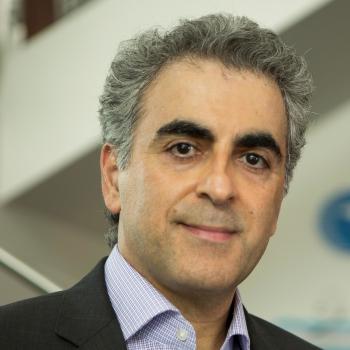 Ali Keshavarzi合作论文数Cypress Semiconductor2
 Ravi M. Todi合作论文数IBM Microelectronics2
 Singh Jagar合作论文数Department of Electrical and Electronic Engineering;Hong Kong University of Sci;Clear Water Bay2Venkata Naresh Mudhireddy合作论文数2Adam Beece合作论文数2
 Dinesh Somasekhar合作论文数2
 Harry J. Levinson合作论文数2Andy Wei合作论文数2
 Ramakanth Alapati合作论文数2R. Nelluri合作论文数1B. Senapati合作论文数1J. Kluth合作论文数1e erben合作论文数1T. Feudel合作论文数1nader magdy hindawy合作论文数1frank barth合作论文数1r asra合作论文数1M-R Lin合作论文数1srikanth b samavedam合作论文数1thomas herrmann合作论文数1Joerg Winkler合作论文数1




