Jan Hoentschel works for GLOBALFOUNDRIES as a Device Manager and is responsible for 28nm low power technologies. He manages an international device engineering team, which is handling several low power CMOS technologies starting from 40nm down to 28nm. Before he was working with Advanced Micro Devices and served several PD-SOI-CMOS device integrations from 130nm down to 32nm technologies for high performance microprocessors. In addition he was working within the product interaction and implementation group at AMD in Austin, TX. Jan Hoentschel is author and co-author of numerous technical papers and patents in the semiconductor field. He holds an MS and PhD in electrical engineering from the Technical University in Dresden as well as an MBA in General Management from the University of Applied Science Bielefeld. His research interests include HKMG, strain engineering, 3D FinFET device and technology concepts, lIIiV semiconductors and low power technologies on CMOS devices.
Continuous process-level and system-level innovation has driven Moore's Law scaling for the last fifty years, and will continue to do so in the next decades. In the last two decades, there has been an acceleration of new materials and devices into semiconductor manufacturing, such as low-k, strained Si, high-k, and FinFET, in order to continue process and cost scaling. At the same time, ever increasing component integration on SoCs has further driven cost scaling, allowing the current mobile era to take shape. In the next decade, the focus of SoC innovation will be on patterning and low-resistance materials on the process side, and multi-die package integration on the system side.
 Jan Hoentschel合作论文数41
 Thorsten Kammler合作论文数AMD;LLC & Co .;AMD Saxony, LLC & Co .33
 Roman Boschke合作论文数18Thilo Scheiper合作论文数18manfred horstmann合作论文数15uwe griebenow合作论文数13
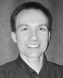 Andreas Gehring合作论文数12casey scott合作论文数10
 Sven Beyer合作论文数9a m waite合作论文数8robert mulfinger合作论文数8anthony mowry合作论文数8peter baars合作论文数7Guillaume Bouche合作论文数7
 Stefan Flachowsky合作论文数7johannes groschopf合作论文数6michael raab合作论文数6
 Tim Baldauf合作论文数6
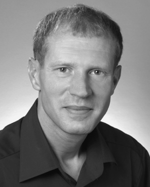 Ralf Illgen合作论文数6Frank Wirbeleit合作论文数Technology Department;Wilschdorfer Landstrasse6jens heinrich合作论文数5maciej wiatr合作论文数5zhenyu hu合作论文数5Manfred Horstmann合作论文数5Peter Javorka合作论文数5
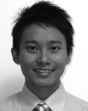 Shao-Ming Koh合作论文数5dae geun yang合作论文数4ralf richter合作论文数4andreas ott合作论文数4qi zhang合作论文数4Martin Trentzsch合作论文数4
 Singh Jagar合作论文数Department of Electrical and Electronic Engineering;Hong Kong University of Sci;Clear Water Bay4
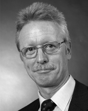 Roland Stenzel合作论文数4jin ping liu合作论文数3markus lenski合作论文数3Ian Cayrefourcq合作论文数3daehan choi合作论文数3h bierstedt合作论文数3gunter grasshoff合作论文数3stefan flachowsky合作论文数3
 Thomas Herrmann合作论文数3hongliang shen合作论文数3
 Daniel Pham合作论文数Department of Radiotherapy, Peter MacCallum Cancer Centre3
 Tom Herrmann合作论文数3Bernhard Trui合作论文数3
 Jing Wan (万景)合作论文数Micro-Nano System Center, School of Information Science and Technology, Fudan University3




