This paper presents a methodology to incorporate and analyze the impact of semiconductor device part-to-part variation on power converter performance. By integrating extensive static and dynamic device characterization data with an automated compact model generation process that reflects manufacturing variability, device models with inherent variability features are utilized in converter simulations for a comprehensive assessment of performance impacts. The traditional converter performance evaluation process typically yields fixed efficiency values, often dismissing the inherent part-to-part variability caused by the manufacturing process of semiconductor devices. To address this limitation, a large population of devices was characterized to capture variations in static parameters-such as transfer, output, and capacitance characteristics-as well as dynamic behaviors, including switching losses. This data-driven approach enables the development of individual compact models, which were then integrated into converter simulations to evaluate efficiency ranges rather than single point estimated values. The converter simulation results show that part-to-part component variation can lead to significant efficiency deviations, exceeding several percentage points in high-power conversion applications. By offering a more accurate representation of converter behavior under real-world manufacturing conditions, this methodology enables designers to anticipate performance variability, improving the robustness of power converter designs.
PN diodes with multi-kilovolt breakdown voltages have been demonstrated to great than 6 kV in GaN, validating the device potential predicted by the intrinsic material properties of III-nitride semiconductors. However, power control circuits also require switching transistors such as junction field effect transistors (JFETs) and practical diodes such as merged PIN Schottky (MPS) diodes. Such devices usually employ selective areas of p-type semiconductor surrounded by n-type material and require the formation of PN junctions with low reverse leakage current. Selective-area p-type doping in Si and SiC based power devices is typically achieved using implantation and thermal annealing to form the p-type areas. Ion implantation of Mg in GaN has demonstrated p-type conductivity, but this process requires specialized equipment for the high-pressure and high-temperature activation of Mg dopants. We have investigated selective-area-regrowth (SArG) to epitaxially grow p-type GaN as an alternative to dopant implantation. Successful PN diode formation by SArG requires a process to remove residual crystalline damage resulting from the ex-situ inductively coupled plasma (ICP) etch typically used to form the p-well, as well as a method to remove the elevated level of Si found at the regrowth interface of a surface that had been exposed to air. For the case of SArG of p-GaN on air-exposed, blanket ICP etched n-type GaN, we present the novel use of a fluorine-based precursor (XeF2) for in-situ etching of GaN in the MOCVD chamber. Unlike chlorine (TBCl and CCl4) and bromine (CBr4) -based precursors we have studied; we obtained a smooth surface following in-situ fluorine etching of air-exposed GaN. Schottky barrier diodes (SBDs) formed by shadow mask evaporation on in-situ fluorine etched n-GaN that had been previously ICP etched showed reverse leakage currents to -40 V that are equal to those of SBDs formed on as-grown n-GaN layers. The in-situ fluorine/ICP etched Schottky diodes had reverse leakage currents more than 3 orders of magnitude lower than those formed on n-GaN layers that had only experienced ICP etching. This suggests that the in-situ fluorine etch was effective at removing the residual damage from the ICP etch process. Furthermore, we discuss the use of in-situ fluorine etching to reduce the concentration of Si at the regrowth interface required to form PN junctions with low reverse leakage current. This work was supported in part by the Advanced Research Projects Agency – Energy (ARPA-E), U.S. Department of Energy under the PNDIODES program directed by Dr. Isik Kizilyalli, and in part by the US Department of Energy (DOE) Vehicle Technologies Office (VTO) under the Electric Drive Train Consortium. Sandia National Laboratories is a multimission laboratory managed and operated by National Technology and Engineering Solutions of Sandia, LLC., a wholly owned subsidiary of Honeywell International, Inc., for the U.S. Department of Energy’s National Nuclear Security Administration under contract DE-NA-0003525. The views expressed in the presentation do not necessarily represent the views of the U.S. Department of Energy or the United States Government.
The use of metal-organic chemical vapor deposition at high temperature is investigated as a means to produce epitaxial hexagonal boron nitride (hBN) at the wafer scale. Several categories of hBN films were found to exist based upon precursor flows and deposition temperature. Low, intermediate, and high NH3 flow regimes were found to lead to fundamentally different deposition behaviors. The low NH3 flow regimes yielded discolored films of boron sub-nitride. The intermediate NH3 flow regime yielded stoichiometric films that could be deposited as thick films. The high NH3 flow regime yielded self-limited deposition with thicknesses limited to a few mono-layers. A Langmuir-Hinshelwood mechanism is proposed to explain the onset of self-limited behavior for the high NH3 flow regime. Photoluminescence characterization determined that the intermediate and high NH3 flow regimes could be further divided into low and high temperature behaviors with a boundary at 1500 degrees C. Films deposited with both high NH3 flow and high temperature exhibited room temperature free exciton emission at 210 nm and 215.9 nm. (C) 2017 Published by Elsevier B.V.
 Luke Yates合作论文数2
 Mary Crawford合作论文数Sandia National Laboratories2
 A. A. Allerman合作论文数Advanced Electronic and Optoelectronic Materials Department, Sandia National Laboratories2Jeffrey Steinfeldt合作论文数1
 Lee Gill合作论文数Sandia National Laboratories, Albuquerque, NM1
 Andrew Binder合作论文数Sandia National Laboratories, Albuquerque, NM, USA1
 Alan J. Michaels合作论文数Bradley Department of Electrical and Computer Engineering, Virginia Polytechnic Institute and State University;Spectrum Dominance Division, Virginia Tech National Security Institute1
 Brianna Klein合作论文数Center for High Technology Materials, University of New Mexico1
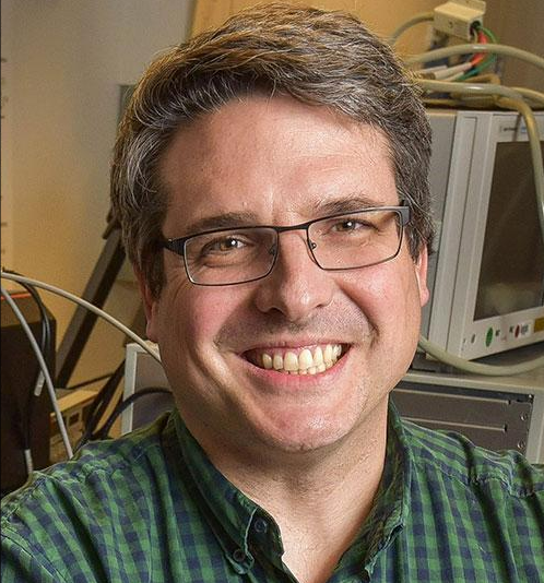 Robert Kaplar合作论文数Department of Energy, Sandia National Laboratories1
 Anthony Rice合作论文数1Taisuke Ohta合作论文数Advanced Light Source;Lawrence Berkeley National Laboratory;Lawrence Berkeley National Laboratory1
 Thomas Beechem合作论文数Engineering Sciences Center, Sandia National Laboratories1Jeffrey J. Figiel合作论文数1Catalin D. Spataru合作论文数Department of Physics;University of California at Berkeley;Department of Physics, University of California at Berkeley1




