A 14-band frequency synthesizer for MB-OFDM UWB using an inductor-less design methodology is presented. It is capable of frequency switching across the entire UWB band in approximately 2 nS, and the phase noise is less than -114 dBc/Hz at 1 MHz offset. Implemented in a 0.13 mu m CMOS technology, the synthesizer dissipates 135 mW from a 1.2 V supply, and occupies only 1.3 mm(2) of silicon area.
A SAW-less dual-band I/Q transmitter without a driver amplifier is designed for dual-band (personal communication system (PCS)/International Mobile Telecommunications (IMT) and cellular) code division multiple access applications. The receive band noise is less than -159 dBc/Hz. It can provide up to + 5-dBm output power and meets the adjacent channel power ratio and dynamic range requirements of both PCS/IMT and cellular CDMA. The measured S 22 is better than -10 dB for both bands and it requires no external matching components. The transmitter is implemented in a 65-nm digital CMOS technology and is packaged using flip-chip technology. The transmitter signal path (RF portion) occupies 1.0 mm 2 .
Injection-locked regenerative frequency dividers can achieve a fractional division ratio similar to regenerative frequency dividers and can provide quadrature output phases. An analysis of the steady-state operation, stability, and phase noise of injection-locked regenerative frequency dividers is presented. In addition, two-stage ring oscillators (based on negative-resistance delay cells) are studied, and their steady-state free-running operation and injection-locked behavior are investigated. Simulation results based on the equations derived in this paper are compared with circuit simulations to examine the accuracy of our analysis, which is quantified in different parts of this paper.
An inductor-less injection-locked frequency divider for high-speed frequency synthesis at V-band is presented. It achieves division by six and operates up to 65 GHz. In addition, it can achieve division ratios of four and two when 44 GHz or 22 GHz input signals are applied, respectively. Implemented in a 0.13 mum digital CMOS technology, the divider draws an average current of 18 mA, and the core area is 0.026 mm2 .
A SAW-less dual-band I/Q transmitter without a Driver Amplifier (DA) is designed for dual-band (PCS/IMT, cellular) CDMA applications. The receive band noise is better than -159 dBc/Hz. It can provide up to +5 dBm output power and meets the ACPR and dynamic range requirements of both PCS/IMT and cellular CDMA. The measured S 22 is better than -10 dB for both bands and it requires no external matching components. The transmitter is implemented in a 65 nm digital CMOS technology, and is packaged using flip-chip technology. The transmitter signal path (RF portion) occupies 1.0 mm 2 .
In this paper a study on different architectures of IF receivers is presented. Existing architectures are compared to suggest the most suitable one for low-voltage low-power wireless applications. Due to limitation of portable equipments, e.g. limited battery life, the main focus lies on the power consumption and integration capability. To have a more practical comparison, the feasibility of removing unnecessary blocks as well as integrating external blocks and components are investigated.
In this paper a 144dB, fourth-order single-loop delta-sigma modulator has been presented with an over-sampling ratio of 1024 and an overload factor of -1.24 dB for a bandwidth of 1000 Rad/s with a new low power integrator in the front-end of the modulator. In this integrator two large mismatch-free capacitors are well embedded to strongly attenuate the input sampling (KT/C) noise without using any large sampling or integrating capacitors. Therefore, the first integrator can be easily designed with a little power and area consumption. Also CDS used in the front-end integrator strongly reduces the 1/f noise and cancels out op-amp's offset. The whole modulator consumes only 8.5 mW from a single 3.0V supply in a 0.6-/spl mu/m CMOS technology.
This paper presents a new compensation method for fully differential two-stage CMOS operational transconductance amplifiers (OTAs). It employs a hybrid cascode compensation scheme, merged Ahuja and improved Ahuja style compensations, for fast settling. A design procedure for minimum settling time of the proposed compensation technique for a two-stage class A/AB OTA is described. To demonstrate the usefulness of it, three design examples are considered.
This paper presents a novel fully-analytical approach to reduce a CMOS NAND gate to an equivalent inverter, based on the modified n-th power law MOSFET model. The series-connected transistors in the NAND gate are converted to an equivalent transistor in a two step process. The proposed model is useful for design automation of complex gates used in VLSI circuits. To show the validity of the technique, the calculated output waveform of the equivalent inverter is compared with that of the NAND gate using HSPICE simulations (level 49).
In this paper, we report the use of the GeneticAlgorithm (GA) to determine the optimum size of theleakage control transistor for low power applications. Inthe optimization, the energy-delay product is minimized.The transistor is modeled by a neural network to increasethe speed and the accuracy of the calculations.
 Lawrence E. Larson合作论文数Brown University11
 Prasad S. Gudem合作论文数Qualcomm Inc.9
 Omid Shoaei合作论文数Department of Electronics, University of Tehran3
 Bhushan Asuri合作论文数3
 Mohammad Yavari合作论文数Integrated Circuits Design Laboratory, Amirkabir University of Technology2
 thomas marra合作论文数1H Zare-Hoseini合作论文数1bhushan shanti asuri合作论文数1junxiong deng合作论文数1thomas andrew myers合作论文数1norman l frederick合作论文数1gurkanwal singh sahota合作论文数1hongyan yan合作论文数1Taherzadeh-S, M.合作论文数1
 Bhagat, M.合作论文数Dept. of Electr. Eng., Rochester Inst. of Technol.;c;Dept. of Electr. Eng., Rochester Inst. of Technol.1Klemens, G.合作论文数1
 Farzam Farbiz合作论文数National University of Singapore1Behnam Amelifard合作论文数University of Southern California;Behnam Amelifard1
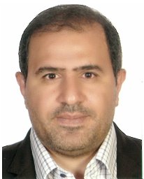 Hossein Imaneini合作论文数College of Engineering, University of Tehran1
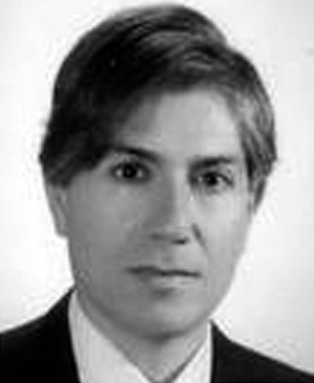 Khosrow Haj Sadeghi合作论文数1
 Hashem Zare-Hoseini合作论文数1
 Ali Afzali-Kusha合作论文数School of Electrical and Computer Engineering, University of Tehran;Low-Power High-Performance Nanosystems and Silicon Intelligence Laboratories, University of Tehran1
 Mohammad Javad Emadi合作论文数1
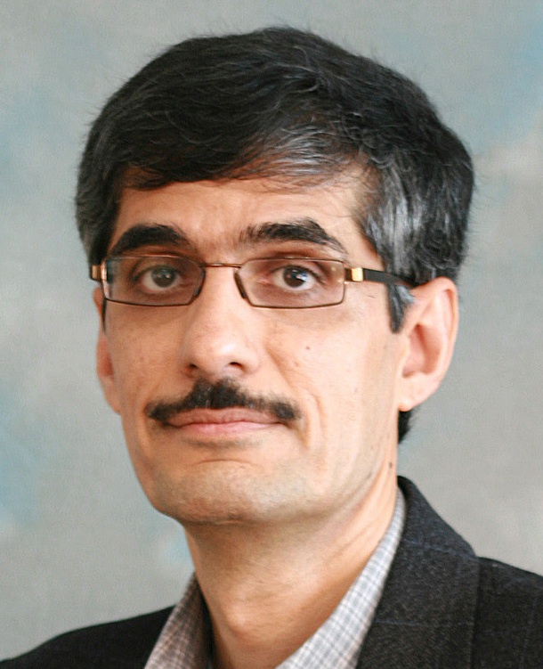 Mehrdad Nourani合作论文数The University of Texas at Dallas;Department of Electrical Engineering1
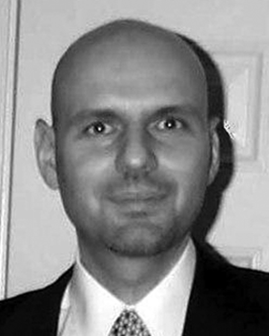 Aristotele Hadjichristos合作论文数1
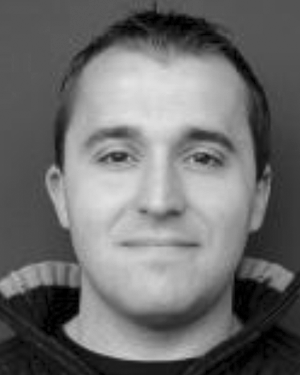 Aleksandar Tasic合作论文数1




