As data transport speed DDR5 supports jumps up to 6.4Gbps, JEDEC requires DFE at DRAM receive as a new equalization feature in evolving specifications. This paper investigates equalization behaviors of DFE and CTLE and their effectiveness at DDR5 operation speeds in varying channel configurations with RDIMM. Relative effects of DFE taps and potential of combined usage with CTLE are studied with eye opening simulations. While margin for operability is subject to device jitter budgets in TX and RX which still are evolving, eye opening margin at 1e-16BER with dual rank RDIMM appears enough for barely over 4Gbps in typical DDR4-like board routing setup and presumptive DDR5 device setup with full crosstalk.
Several designs of High-Bandwidth Memory (HBM) interface have been reported so far, all on silicon interposer. With the promise of organic interposer to become a lower-cost alternative, complete understanding of electrical performance of such interface is required. HBM interface connects SoC (System on Chip) and HBM dies that are placed next to each other on a common substrate; therefore, it is only a few millimeters long. With all eight channels routed, it counts close to 1700 signals that run on three layers, as limited by today's process technology. As the HBM die and, subsequently, the interface width is only 6 millimeters, these signals have to be routed with very high density. This results in high crosstalk. Specific to the organic interface, the short HMB signal lines, in combination with the driver complex-valued output impedance and the capacitive input of the receiver, creates under-dampened LC(R) tank resonators circuit with natural frequency of oscillation around 3-4 GHz. Even a weak crosstalk excitation from an adjacent aggressor signals causes a quiet victim signal to undergo resonant oscillation, or ringing. The coupling between adjacent signals even within the breakout area is severe enough to reduce noise margins to zero. The resistive loss in signal traces must be sufficient to dampen this ringing. We consider various technology options to increase the loss and compare their relative efficacy. Two distinct types of crosstalk are identified and their respective effect on HBM2 timing and noise margin is discussed. Effects of the meshed (a.k.a. perforated) reference plane on intra -and interlayer crosstalk is studied. With the trace cross-sectional dimensions at 2x2um and Nyquist frequency of 1GHz, the signals operate at the onset of skin effect, with per-unit-length resistance and inductance undergoing severe dispersion. This differs from signals routed as wider traces on an organic package, where the skin effect develops at much lower frequencies. It is also in sharp contrast to on-die signal routing, where RC is an adequate model of the signal interconnect.
This paper discusses multi-point address channel design in fly-by topology for high speed memory interface. Waveform behaviors at DRAM locations along the channel are examined in depth with eye opening data in various channel design factors and device termination settings. Eye opening is exacerbated on the front DRAM from the controller more prominently due to ring-backs from high frequency reflections at the node while eye opening at DRAMs along mid-channel is more notably affected by dual eye tracks from effective channel impedance to termination mismatch as well as high frequency loss from DRAM nodes of channel front. Channel design is explored for overall channel performance improvement to consider different waveform behaviors at address input nodes of multiple DRAMs along the channel and design suggestions are developed.
Voltage supply noise can impact circuit system performance and functionality. FPGA (Field Programmable Gate Arrays) applications vary from different usage model, the detection of supply noise is crucial for these applications. Detection sensitivity is directly related to detector stage delay. This paper discusses the detector stage delay versus sensitivity relationship. It also demonstrates a novel technique to improve the detector stage delay by interpolations. An implementation example of time digital converter using the original method and the interpolation method in FPGA fabric is also demonstrated and compared.
In high density, high speed Serdes interconnect designs, inappropriate pin placement can lead to differential crosstalk violation. How to relatively compare the crosstalk level due to various pin placements, and estimate its effect on the whole system without time consuming simulation is critical. This paper introduces a simple method to estimate the relative differential crosstalk due to various pin distributions. The effectiveness of this method is investigated using commercial 3D electromagnetic software. How the surrounding environment can affect the crosstalk level is also studied in this article.
This paper discusses link routing budget considerations for PCIe Gen3 designs in server systems. Special attention will be given to channel discontinuities and their effect on eye opening. Link training complications will be discussed with respect to equalization and tuning behavior when accommodating multiple transmitters and receivers from different vendor sources. Insertion loss plots and eye simulation data will be analyzed and interpreted. Hardware data will show that optimally simulated equalization cases may not necessarily occur.
This paper introduces a novel air-dielectric via structure which can improve the interconnect signal bandwidth by reducing the impedance mismatch in vias of high speed system PCBs carrying 20 Gbps+ signals. Design methods of the proposed air-dielectric structure are presented. Using these methods a system target design impedance can be better matched thus causing reductions in the signal degradation caused by the reflections as well as propagation losses.
This paper discusses the impact of DC wander also called baseline wander resulting from AC-coupling on signal integrity in receive waveforms in AC-coupled serial bus links with focus on PCIe Gen3 signaling. Receive signal behavior from charging and discharging activities of AC-coupling circuit is studied for fundamental understanding of baseline wander and its effect through simulations of short and long channels from various aspects of PCIe Gen3 signaling and high speed serial links in general.
This study presents a dielectric waveguide via design. The design serves two purposes. First, it removes the need for DC-blocking capacitors within a high speed signaling system. This is because it is free of conductors and made of dielectric materials thus inherently accomplishing DC-blocking on a signal travel route. Second, it allows for efficient via performance at millimeter wave frequencies which is harder to achieve using traditional metallic via designs. The design uses quasi-optical principles in order to make the transit between one PCB layer trace to another possible. This study presents the design guidelines for such a via along with simulations showing operation and evaluating performance.
As DDR4 continues to move from the design phase towards implementation, several challenges have been identified to successfully implement this high performance memory architecture for next generation systems. This paper investigates driver design selection for DDR4 systems. The paper studies the pros and cons of three driver design types namely: standard, pre-emphasis, and de-emphasis on typical net topogies of 1DPC (DIMM per channel) and 2DPC operated at 2400MT/s. For each driver type the impact of source termination on performance and power saving capability is discussed. Since the effects associated with different driver designs can be best understood in the time domain this paper uses behavioral models created in the SPICE format for simulations.
 Madhavan Swaminathan合作论文数School of Materials Science and Engineering, Georgia Institute of Technology;Center for Heterogeneous Integration of Micro Electronic Systems, College of Engineering, The Pennsylvania State University7
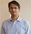 Bhyrav M Mutnury合作论文数Dell EMC6
 Moises Cases合作论文数IBM Corporation6
 lloyd a walls合作论文数5d zwitter合作论文数5J. Audet合作论文数5
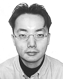 Sungjun Chun合作论文数4Nam Pham合作论文数4Haitian Hu合作论文数4Jin Woo Hong合作论文数Department of Electrical and Computer Engineering
Louisiana State University4
Sungjun Chun合作论文数4Nam Pham合作论文数4Haitian Hu合作论文数4Jin Woo Hong合作论文数Department of Electrical and Computer Engineering
Louisiana State University4 Jose A. Hejase合作论文数4tae hong kim合作论文数3Yonehara, K.合作论文数3Choi, K.L.合作论文数3Daniel M. Dreps合作论文数IBM System and Technology Group, Austin, TX, USA3m arseneault合作论文数2
 n pham合作论文数2Changyi Su合作论文数2Sean Long合作论文数2Hong Shi合作论文数2Juan Wang合作论文数2Shen Dong合作论文数2Rohan Mandrekar合作论文数2
 Yong Wang合作论文数Sch. of Electr. & Electron. Eng., Nanyang Technol. Univ.;c;Sch. of Electr. & Electron. Eng., Nanyang Technol. Univ.2Gary Lafontant合作论文数2
 Anand Haridass合作论文数2Yaping Zhou合作论文数2andrea paganini合作论文数1ivan l wemple合作论文数1terence rodrigues合作论文数1eric w tremble合作论文数1Libous, J.P.合作论文数1
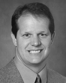 paul m harvey合作论文数1si t win合作论文数1
 Daniel Rodriguez Gutierrez合作论文数Department of Endocrinology, Metabolism and Cardiovascular System, University of Fribourg1charles chiu合作论文数1Thomas To合作论文数Xilinx Inc, 2100 Log Dr, San Jose, CA 95124 USA1Baumgartner, S.合作论文数1Tao Wang合作论文数1Dunham, D.合作论文数1Xin Wu合作论文数1Roger D Weekly合作论文数1Levesque, R.合作论文数1Pharand, S.合作论文数1Mandrekar, R.合作论文数1Budell, T.合作论文数1R. E. Anderson合作论文数1Daniel O'Connor合作论文数1
 Mark J Bailey合作论文数NERC Institute of Virology and Environmental Microbiology, Mansfield Road, Oxford OX1 3SR, UK1




