High-performance photonic chips provide a powerful platform for analog computing, enabling the simulation of high-dimensional physical systems using low-dimensional devices with additional synthetic dimensions. The realization of large-scale complex simulations necessitates an architecture capable of rich coupling configurations (encompassing symmetric, asymmetric and long-range coupling schemes) which is also crucial for scaling up. Previous approaches rely on excessive physical components to introduce asymmetric coupling, however, are restricted in reconfiguring and scaling by the relatively complicated structures. Here, to solve this problem, we propose a hybrid-frequency synthetic-dimension simulator architecture that combines both intra-resonant and inter-resonant frequency-lattice sites, and experimentally demonstrate it using the thin-film lithium niobate (TFLN) photonic chip. Employing this hybrid programmable architecture, we are able to simulate both the regular and long-range coupled forms of diverse compound-lattice models, such as the Hall ladder, Creutz ladder (symmetric) and Su-Schrieffer-Heeger (SSH, asymmetric) model, on a single chip, simultaneously reducing the experimental requirements significantly. As results, the direct readout of the bandstructure of the SSH model is able to be achieved, to be distinguished from all previous works, and important phenomena such as spin-momentum locking, topological flat band and Aharonov-Bohm cage effect are also observed with lower experimental requirements. Furthermore, applications like piecewise-continuous optical frequency shifting can be enabled by cascading our devices. Our results offer promising insights for future large-scale complex on-chip simulators with rich couplings.
Vortex beams carrying orbital angular momentum have attracted increasing attention due to the helical wavefront, extensive high-dimensional state space, and cross-disciplinary applicability in fields such as high-capacity optical communication, optical manipulation, and super-resolution optical imaging. However, the intensity profile of vortex beams exhibits a topological charge-dependent annular structure, which imposes fundamental constraints on wavefront modulation flexibility, particularly in multi-mode coupling systems. In this study, we report a switchable perfect vortex beam (PVB) generator with high efficiency in the visible by combining spatially patterned photoalignment of nematic liquid crystal (LC) with multiplexed geometric phase profiles. Comprehensive simulations and experimental characterization demonstrate that the LC geometric-phase-based PVB generator produces high-quality vortex beams with spatially invariant intensity profiles across topological charges ranging from l = - 8 to + 8 and with an average conversion efficiency up to 86%. Moreover, we reveal that the PVB generator is switchable between left- and right-handed circularly polarized beams. This study demonstrates the feasibility of generating high-quality PVB through highly integrated flat LC photonic device, and may find applications in OAM multiplexing in quantum communication networks and ultrahigh-capacity photonic interconnects.
High-performance photonic chips provide a powerful platform for analog computing, enabling the simulation of high-dimensional physical systems using low-dimensional devices with additional synthetic dimensions. The realization of large-scale complex simulations necessitates an architecture capable of arbitrary coupling configurations (encompassing symmetric, asymmetric and long-range coupling schemes) which is also crucial for scaling up. Previous approaches rely on excessive physical components to introduce asymmetric coupling, however, are restricted in reconfiguring and scaling by the relatively complicated structures. Here, to solve this problem, we propose a hybrid-frequency synthetic-dimension simulator architecture that combines both intra-resonant and inter-resonant frequency-lattice sites, and experimentally demonstrate it using the thin-film lithium niobate (TFLN) photonic chip. Employing this hybrid programmable architecture, we are able to simulate both the regular and long-range coupled forms of diverse compound-lattice models, such as the Hall ladder, Creutz ladder (symmetric) and Su-Schrieffer-Heeger (SSH, asymmetric) model, on a single chip, simultaneously reducing the experimental requirements significantly. As results, the direct readout of the bandstructure of the SSH model is able to be achieved, to be distinguished from all previous works, and important phenomena such as spin-momentum locking, topological flat band and Aharonov-Bohm cage effect are also observed with lower experimental requirements. Furthermore, applications like piecewise-continuous optical frequency shifting can be enabled by cascading our devices. Our results offer promising insights for future large-scale complex on-chip simulators with arbitrary couplings.
Optical fiber integrated devices have attracted increasing attention due to its advantages of small size, and high-degree integration of diverse functionalities. Traditional fiber integrated devices are usually composed of dielectric or metallic microstructures, which rely on expensive and complex lithography process. Moreover, the functionality of fiber optics with static and fixed geometry is unadjustable, which greatly limits their applications. In this article, we design and demonstrate an optical fiber end-facet integrated liquid crystal (LC) photonic devices for beam shaping. The LC polymer droplets with planar and homeotropic anchoring on the single-mode fiber end-facet were prepared to realize the beam shaping devices in the visible. These two kind of LC polymer droplets with special director configurations were simulated using Q-tensor model and Rayleigh-Sommerfeld diffraction theory. The optical properties of the LC polymer droplets under different anchoring conditions were experimentally verified. The experimental results match the simulation results, thus proving the beam shaping ability of the LC devices. This study provides a new approach to realize compact and integrated optical fiber optics with lower cost and high efficiency.
Quantum networks provide a prospective paradigm to connect separated quantum nodes, which relies on the distribution of long-distance entanglement and active feedforward control of qubits between remote nodes. Such approaches can be utilized to construct nonlocal quantum gates, forming building blocks for distributed quantum computing and other novel quantum applications. However, these gates have only been realized within single nodes or between nodes separated by a few tens of meters, limiting the ability to harness computing resources in large-scale quantum networks. Here, we demonstrate nonlocal photonic quantum gates between two nodes spatially separated by 7.0 km using stationary qubits based on multiplexed quantum memories, flying qubits at telecom wavelengths, and active feedforward control based on field-deployed fibers. Furthermore, we illustrate quantum parallelism by implementing the Deutsch-Jozsa algorithm and the quantum phase estimation algorithm between the two remote nodes. These results represent a proof-of-principle demonstration of quantum gates over metropolitan-scale distances and lay the foundation for the construction of large-scale distributed quantum networks relying on existing fiber channels. Full-fledged quantum communication networks would allow distributed quantum computing across multiple remote nodes, but typical implementations are stuck at meters-scale distances. Here the authors demonstrate teleportation-based nonlocal CNOT gates, distributed Deutsch-Jozsa algorithm and quantum phase estimation across 7 km space separation.
Liquid crystal (LC) photonic devices have attracted intensive attention in recent decades, due to the merits of tunability, cost-effectiveness, and high efficiency. However, the precise and efficient simulation of large-scale three-dimensional electrically stimulated LC photonic devices remains challenging and resource consuming. Here we report a straightforward nonuniform finite difference method (NFDM) for efficiently simulating large-scale LC photonic devices by employing a spatially nonuniform mesh grid. We show that the NFDM can be further accelerated by approximately 504 times by using the improved successive over-relaxation method (by 12 times), the symmetric boundary (by 4 times), the momentum gradient descent algorithm (by 3.5 times), and the multigrid (by 3 times). We experimentally fabricated the large-scale electrically stimulated LC photonic device, and the measured results demonstrate the effectiveness and validity of the proposed NFDM. The NFDM allocates more grids to the core area with steep electric field gradient, thus reducing the distortion of electric field and the truncation error of calculation, rendering it more precise than the finite element method and traditional finite difference method with similar computing resources. This study demonstrates an efficient and highly reliable method to simulate the large-scale electrically stimulated LC photonic device, and paves the way for customizing a large-scale LC photonic device with designable functionalities.
Vortex beams have attracted extensive attention in recent decade due to the carried optical orbital angular momentum (OAM). Vortex beams carrying different OAM modes are orthogonal to each other, and thus have become highly promising in realizing high-capacity optical communication systems. This review is to introduce the fundamental principles of optical OAM mode demultiplexing, recent advances in the fabrication techniques and emerging applications in high-capacity optical communications. First, this review introduces the development history of the working principle of OAM mode demultiplexer. Subsequently, a variety of preparation techniques and emerging applications of OAM mode demultiplexing are discussed in detail. Finally, we provide an in-depth analysis and outlook for the future trends and prospects of the OAM mode demultiplexer.
The implementation of scalable quantum networks requires photons at the telecom band and long-lived spin coherence. The single Er 3+ in solid-state hosts is an important candidate that fulfills these critical requirements simultaneously. However, to entangle distant Er 3+ ions through photonic connections, the emission frequency of individual Er 3+ in solid-state matrix must be the same, which is challenging because the emission frequency of Er 3+ depends on its local environment. Herein, we propose and experimentally demonstrate the Stark tuning of the emission frequency of a single Er 3+ in a Y 2 SiO 5 crystal by employing electrodes interfaced with a silicon photonic crystal cavity. We obtain a Stark shift of 182.9±0.8 MHz, which is approximately 27 times of the optical emission linewidth, demonstrating promising applications in tuning the emission frequency of independent Er 3+ into the same spectral channels. Our results provide a useful solution for construction of scalable quantum networks based on single Er 3+ and a universal tool for tuning emission of individual rare-earth ions.
Quantum memories at telecom wavelengths are crucial for the construction of large-scale quantum networks based on existing fiber networks. On-demand storage of telecom photonic qubits is an essential request for such networking applications but yet to be demonstrated. Here we demonstrate the storage and on-demand retrieval of telecom photonic qubits using a laser-written waveguide fabricated in an ^{167}Er^{3+}:Y_{2}SiO_{5} crystal. Both ends of the waveguide memory are directly connected with fiber arrays with a fiber-to-fiber efficiency of 51%. Storage fidelity of 98.3(1)% can be obtained for time-bin qubits encoded with single-photon-level coherent pulses, which is far beyond the maximal fidelity that can be achieved with a classical measure and prepared strategy. This device features high reliability and easy scalability, and it can be directly integrated into fiber networks, which could play an essential role in fiber-based quantum networks.
Er3+:Y2SiO5 is a material of particular interest due to its suitability for telecom-band quantum memories and quantum transducers interfacing optical communication with quantum computers working in the microwave regime. Extending the coherence lifetimes of the electron spins and the nuclear spins is essential for implementing efficient quantum information processing based on such hybrid electron-nuclear spin systems. The electron spin coherence time of Er3+:Y2SiO5 is so far limited to several microseconds, and there are significant challenges in optimizing coherence lifetimes simultaneously for both the electron and nuclear spins. Here we perform a pulsed-electron-nuclear-double-resonance investigation for an Er3+-doped material at subkelvin temperatures. At the lowest working temperature, the electron spin coherence time reaches 290 ?? 17 ??s, which has been enhanced by 40 times compared with the previous results. In the subkelvin regime, a rapid increase in the nuclear spin coherence time is observed, and the longest coherence time of 738 ?? 6 ??s is obtained. These extended coherence lifetimes could be valuable resources for further applications of Er3+:Y2SiO5 in fiber-based quantum networks.
Due to the inevitable loss of single photon transmission in optical fiber, a quantum repeater scheme is needed to establish large-scale quantum networks. The existing elementary quantum repeater links are all based on emissive quantum memories, with entangled photons emitted by the memory itself. This architecture is difficult to support deterministic photon emission and multiplexing storage simultaneously, which fundamentally limits the rate of entanglement distribution. In this talk, I will present our recent work about the realization of heralded quantum entanglement between two absorptive quantum memories based on rare-earth-ion-doped crystals. This work confirmed the feasibility of constructing quantum repeater based on absorptive quantum memories and demonstrated the acceleration effect of multiplexing in quantum repeater for the first time, which lays a solid foundation for the construction of practical high-speed quantum networks.
${\mathrm{Er}}^{3+}\text{:}{\mathrm{Y}}_{2}{\mathrm{SiO}}_{5}$ is a material of particular interest due to its suitability for telecom-band quantum memories and quantum transducers interfacing optical communication with quantum computers working in the microwave regime. Extending the coherence lifetimes of the electron spins and the nuclear spins is essential for implementing efficient quantum information processing based on such hybrid electron-nuclear spin systems. The electron spin coherence time of ${\mathrm{Er}}^{3+}\text{:}{\mathrm{Y}}_{2}{\mathrm{SiO}}_{5}$ is so far limited to several microseconds, and there are significant challenges in optimizing coherence lifetimes simultaneously for both the electron and nuclear spins. Here we perform a pulsed-electron-nuclear-double-resonance investigation for an ${\mathrm{Er}}^{3+}$-doped material at subkelvin temperatures. At the lowest working temperature, the electron spin coherence time reaches 290 $\ifmmode\pm\else\textpm\fi{}$ 17 $\mathrm{\ensuremath{\mu}}\mathrm{s}$, which has been enhanced by 40 times compared with the previous results. In the subkelvin regime, a rapid increase in the nuclear spin coherence time is observed, and the longest coherence time of 738 $\ifmmode\pm\else\textpm\fi{}$ 6 $\mathrm{\ensuremath{\mu}}\mathrm{s}$ is obtained. These extended coherence lifetimes could be valuable resources for further applications of ${\mathrm{Er}}^{3+}\text{:}{\mathrm{Y}}_{2}{\mathrm{SiO}}_{5}$ in fiber-based quantum networks.
Duan-Cheng Liu, 2, ∗ Pei-Yun Li, 2, ∗ Tian-Xiang Zhu, 2 Liang Zheng, 2 Jian-Yin Huang, 2 Zong-Quan Zhou, 2, † Chuan-Feng Li, 2, † and Guang-Can Guo 2 CAS Key Laboratory of Quantum Information, University of Science and Technology of China, Hefei, 230026, China CAS Center for Excellence in Quantum Information and Quantum Physics, University of Science and Technology of China, Hefei, 230026, China (Dated: January 12, 2022)
Entanglement distillation is an essential ingredient for long-distance quantum communication. However, owing to their demanding requirements, integrating such entanglement distillation processing in scalable quantum devices remains an outstanding challenge. Here we propose the implementation of the filtering protocol in atomic ensembles, which are promising candidates for building quantum repeater nodes, and analyze the boost entanglement distribution rate considering different scenarios. Moreover, we demonstrate the key step of this approach with a proof-of-principle experiment in a rare-earth-ion-doped crystal ( 143 Nd 3+ :Y 2 SiO 5 ). Leveraging its multi-level structure and long-lived coherence, spin manipulations are implemented with an average fidelity exceeding 97.2%, leading to the preparation of entanglement between the electron and nuclear spins with a concurrence of 0.75 with a sample temperature of 100 mK. The versatility, robustness, and potential scalability of our proposal contribute to the construction of quantum repeaters and quantum networks based on atomic ensembles.
Er 3+ :Y 2 SiO 5 is a material of particular interest due to its suitability for telecom-band quantum memories and quantum transducers interfacing optical communication with quantum computers working in the microwave regime. Extending the coherence lifetimes of the electron spins and the nuclear spins is essential for implementing efficient quantum information processing based on such hybrid electron-nuclear spin systems. The electron spin coherence time of Er 3+ :Y 2 SiO 5 is so far limited to several microseconds, and there are significant challenges in optimizing coherence lifetimes simultaneously for both the electron and nuclear spins. Here we perform a pulsed-electron-nuclear-double-resonance investigation for an Er 3+ -doped material at subkelvin temperatures. At the lowest working temperature, the electron spin coherence time reaches 290 ± 17 µ s, which has been enhanced by 40 times compared with the previous results. In the subkelvin regime, a rapid increase in the nuclear spin coherence time is observed, and the longest coherence time of 738 ± 6 µ s is obtained. These extended coherence lifetimes could be valuable resources for further applications of Er 3+ :Y 2 SiO 5 in fiber-based quantum networks.
Er:Y2SiO5 at Sub-Kelvin Temperatures Jian-Yin Huang, 2 Pei-Yun Li, 2 Zong-Quan Zhou, 2, ∗ Chuan-Feng Li, 2, † and Guang-Can Guo 2 CAS Key Laboratory of Quantum Information, University of Science and Technology of China, Hefei, 230026, China CAS Center For Excellence in Quantum Information and Quantum Physics, University of Science and Technology of China, Hefei, 230026, China (Dated: July 12, 2021)
Owing to the inevitable loss in communication channels, the distance of entanglement distribution is limited to approximately 100 kilometres on the ground 1 . Quantum repeaters can circumvent this problem by using quantum memory and entanglement swapping 2 . As the elementary link of a quantum repeater, the heralded distribution of two-party entanglement between two remote nodes has only been realized with built-in-type quantum memories 3 – 9 . These schemes suffer from the trade-off between multiplexing capacity and deterministic properties and hence hinder the development of efficient quantum repeaters. Quantum repeaters based on absorptive quantum memories can overcome such limitations because they separate the quantum memories and the quantum light sources. Here we present an experimental demonstration of heralded entanglement between absorptive quantum memories. We build two nodes separated by 3.5 metres, each containing a polarization-entangled photon-pair source and a solid-state quantum memory with bandwidth up to 1 gigahertz. A joint Bell-state measurement in the middle station heralds the successful distribution of maximally entangled states between the two quantum memories with a fidelity of 80.4 ± 2.2 per cent (±1 standard deviation). The quantum nodes and channels demonstrated here can serve as an elementary link of a quantum repeater. Moreover, the wideband absorptive quantum memories used in the nodes are compatible with deterministic entanglement sources and can simultaneously support multiplexing, which paves the way for the construction of practical solid-state quantum repeaters and high-speed quantum networks.
An experimental platform of ultralow-temperature pulsed ENDOR (electron-nuclear double resonance) spectroscopy is constructed for the bulk materials. Coherent property of the coupled electron and nuclear spins of the rare-earth (RE) dopants in a crystal (143Nd3+:Y2SiO5) is investigated from 100 mK to 6 K. At the lowest working temperatures, two-pulse-echo coherence time exceeding 2 ms and 40 ms are achieved for the electron and nuclear spins, while the electronic Zeeman and hyperfine population lifetimes are more than 15 s and 10 min. With the aid of the near-unity electron spin polarization at 100 mK, the complete hyperfine level structure with 16 energy levels is measured using ENDOR technique without the assistance of the reconstructed spin Hamiltonian. These results demonstrate the suitability of the deeply cooled paramagnetic RE-doped solids for memory components aimed for quantum communication and quantum computation. The developed experimental platform is expected to be a powerful tool for paramagnetic materials from various research fields.
$\mathrm {^{151}Eu^{3+}}$-doped yttrium silicate ($\mathrm {^{151}Eu^{3+}:Y_2SiO_5}$ ) crystal is a unique material that possesses hyperfine states with coherence time up to 6 h. Many efforts have been devoted to the development of this material as optical quantum memories based on the bulk crystals, but integrable structures (such as optical waveguides) that can promote $\mathrm {^{151}Eu^{3+}:Y_2SiO_5}$-based quantum memories to practical applications, have not been demonstrated so far. Here we report the fabrication of type 2 waveguides in a $\mathrm {^{151}Eu^{3+}:Y_2SiO_5}$ crystal using femtosecond-laser micromachining. The resulting waveguides are compatible with single-mode fibers and have the smallest insertion loss of $4.95\ dB$. On-demand light storage is demonstrated in a waveguide by employing the spin-wave atomic frequency comb (AFC) scheme and the revival of silenced echo (ROSE) scheme. We implement a series of interference experiments based on these two schemes to characterize the storage fidelity. Interference visibility of the readout pulse is $0.99\pm 0.03$ for the spin-wave AFC scheme and $0.97\pm 0.02$ for the ROSE scheme, demonstrating the reliability of the integrated optical memory.
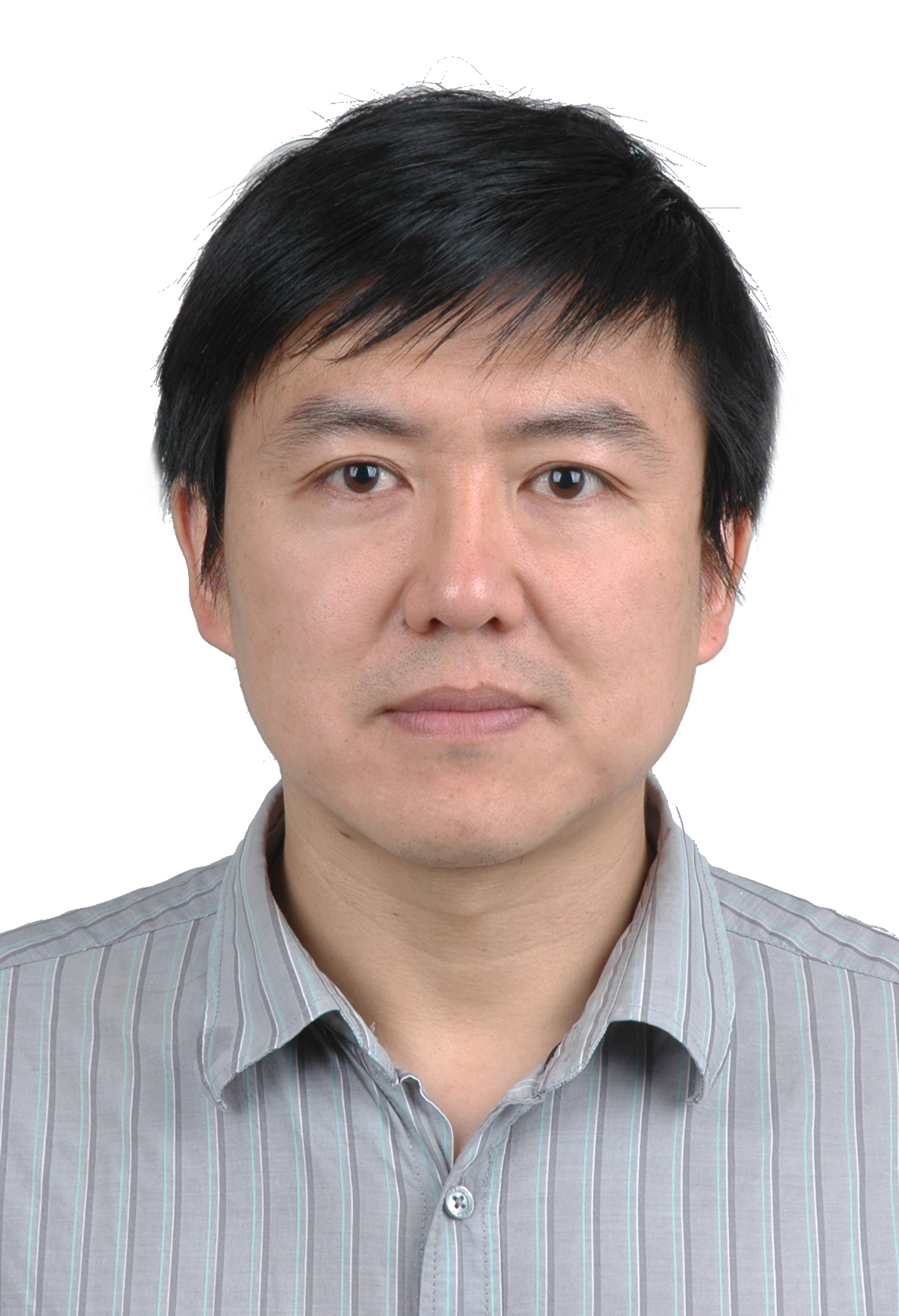 Chuan-Feng Li (李传锋)合作论文数University of Science and Technology of China;Key Laboratory of Quantum Information, Chinese Academy of Sciences24
 Zongquan Zhou (周宗权)合作论文数School of Physical Sciences, University of Science and Technology of China23
 Guangcan Guo (郭光灿)合作论文数School of Physical Sciences, University of Science and Technology of China;Key Lab of Quantum Information, Chinese Academy of Sciences, University of Science and Technology of China21
 Xiao Liu (刘晓)合作论文数School of Physics, University of Electronic Science and Technology of China14
 Jian-Yin Huang合作论文数10Peng-Jun Liang合作论文数Univ Sci & Technol China, CAS Key Lab Quantum Informat, Hefei 230026, Anhui, Peoples R China10
 Chao Liu合作论文数Univ Sci & Technol China, CAS Key Lab Quantum Informat, Hefei 230026, Peoples R China10Yu Ma合作论文数8
 Tian-Shu Yang合作论文数Univ Sci & Technol China, CAS Key Lab Quantum Informat, Hefei 230026, Anhui, Peoples R China8
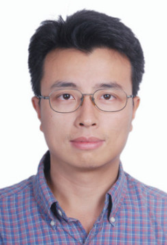 Jun Hu (胡军)合作论文数苏州大学物理科学与技术学院7
 Li Xue (薛力)合作论文数College of Physical Science and Technology, Xiamen University7Li Zong-Feng合作论文数6Tian-Xiang Zhu合作论文数6
 Andy Chong合作论文数Department of Applied Physics;Cornell University;Department of Applied Physics, Cornell University6Yi-Lin Hua合作论文数Univ Sci & Technol China, CAS Key Lab Quantum Informat, Hefei 230026, Peoples R China5Liang Zheng合作论文数5
 Tu Tao (涂涛)合作论文数Department of Optics and Optical Engineering, School of Physical Sciences, University of Science and Technology of China5Yi-Xin Xiao合作论文数4
 Qian Cao合作论文数Dept Phys, Univ Hamburg4
 Yun Zhao合作论文数Dept Elect Engn, Columbia Univ4
 Huapeng Ye (叶华朋)合作论文数South China Academy of Advanced Optoelectronics, South China Normal University4
 Guofu Zhou (周国富)合作论文数South China Academy of Advanced Optoelectronics, South China Normal University4Duan-Cheng Liu (刘端程)合作论文数3Chenchen Wan合作论文数3Han Li合作论文数3
 Dong Yuan (袁冬)合作论文数South China Academy of Advanced Optoelectronics, South China Normal University3
 Zongfeng Li (李宗峰)合作论文数University of Chinese Academy of Sciences3
 Yongjian Han (韩永建)合作论文数School of Physical Sciences, University of Science and Technology of China;Chinese Academy of Sciences3
 Partha Banerjee合作论文数Department of Electro-Optics and Photonics, School of Engineering, University of Dayton3
 Jin-Shi Xu (许金时)合作论文数School of Physical Sciences, University of Science and Technology of China3
 Jianshun Tang (唐建顺)合作论文数School of Physical Sciences, University of Science and Technology of China3Zhenghao Guo合作论文数2Xi-Wang Luo合作论文数Univ Texas Dallas, Dept Phys, Richardson, TX 75080 USA2Zhao-An Wang合作论文数2
 Xiao-Dong Zeng合作论文数CAS, Univ Sci & Technol China2
 Ming Jin合作论文数2
 Wei Liu (刘伟)合作论文数School of Chemistry & Chemical Engineering, Shaanxi Normal University2
 Shuang Wang (王双)合作论文数Chinese Academy of Sciences;University of Science and Technology of China2
 Yang Mu (穆杨)合作论文数School of Environment, University of Science and Technology of China2
 Xin Huang (黄昕)合作论文数Institute of Remote Sensing Information Processing, School of Remote Sensing and Information Engineering, Wuhan University2
 Diane Beamer合作论文数1Jia-Le Miao合作论文数1
 Mengjun Liu合作论文数1
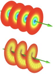 Rudra Gnawali合作论文数Appl Optimizat Inc1
 Akash Kota合作论文数Dept Elect & Comp Engn, Univ Dayton1
 Ruizhi Yang合作论文数1You-Zhi Ma合作论文数1Xing-Yu Zhu合作论文数Univ Sci & Technol China, Chinese Acad Sci, Key Lab Quantum Informat, Hefei 230026, Anhui, Peoples R China1Xinyu Yang合作论文数1




