High-performance photonic chips provide a powerful platform for analog computing, enabling the simulation of high-dimensional physical systems using low-dimensional devices with additional synthetic dimensions. The realization of large-scale complex simulations necessitates an architecture capable of rich coupling configurations (encompassing symmetric, asymmetric and long-range coupling schemes) which is also crucial for scaling up. Previous approaches rely on excessive physical components to introduce asymmetric coupling, however, are restricted in reconfiguring and scaling by the relatively complicated structures. Here, to solve this problem, we propose a hybrid-frequency synthetic-dimension simulator architecture that combines both intra-resonant and inter-resonant frequency-lattice sites, and experimentally demonstrate it using the thin-film lithium niobate (TFLN) photonic chip. Employing this hybrid programmable architecture, we are able to simulate both the regular and long-range coupled forms of diverse compound-lattice models, such as the Hall ladder, Creutz ladder (symmetric) and Su-Schrieffer-Heeger (SSH, asymmetric) model, on a single chip, simultaneously reducing the experimental requirements significantly. As results, the direct readout of the bandstructure of the SSH model is able to be achieved, to be distinguished from all previous works, and important phenomena such as spin-momentum locking, topological flat band and Aharonov-Bohm cage effect are also observed with lower experimental requirements. Furthermore, applications like piecewise-continuous optical frequency shifting can be enabled by cascading our devices. Our results offer promising insights for future large-scale complex on-chip simulators with rich couplings.
The negatively charged boron vacancy in two-dimensional hexagonal boron nitride has emerged as a promising candidate for quantum sensing. The coherence time of this defect spins which coherent quantum sensing resides in is limited spin-phonon interactions, while the underlying physical mechanism of the corresponding high-temperature behavior is still not fully understood. Here, we probe the single- and double-quantum relaxation rates on this center over the temperature range from 293 to 393 K. The results show that both relaxation rates increase with increasing temperature, and the double-quantum relaxation rate significantly increases rapidly. At high temperature (above 400 K), the double-quantum relaxation rate is much greater than single-quantum relaxation rate, and may dominate the decoherence channel of spin-phonon interactions. Using a theoretical model of second-order spin-phonon interactions, we attribute the high-temperature spin relaxation rates to interactions with higher-energy effective phonon mode, aiding the further understanding and guiding high-temperature sensing applications.
ABSTRACT Exceptional points (EPs), as an essential concept in non‐Hermitian systems, give rise to a variety of novel physical phenomena, most notably the exchange of eigenstates induced by encircling in parameter space. Here, we experimentally investigate eigenstate permutations in a parameter space containing three second‐order exceptional points (EP2s), realized on a programmable single‐photon platform capable of synthesizing four‐state non‐Hermitian Hamiltonians. By designing distinct parameter space loops that encircle the EP2s in different sequences, we observe eigenvalue and eigenstate permutations corresponding to the non‐Abelian dihedral group. Furthermore, using a branch‐cut representation of the underlying Riemann‐surface topology, we track the associated eigenstate permutations and show that different encircling paths generate distinct sequences of permutation operations. These results highlight the non‐commutative nature of eigenstate braiding in multi‐EP systems and establish an experimental connection between multi‐EP topology and non‐Abelian group structures in non‐Hermitian physics. More broadly, our work demonstrates the capability of programmable single‐photon platforms for investigating complex non‐Hermitian topological structures and their associated permutation dynamics.
Investigating physical models with photonic synthetic dimensions has been generating great interest in vast fields of science. The rapidly developing thin-film lithium niobate (TFLN) platform, for its numerous advantages including high electro-optic coefficient and scalability, is well compatible with the realization of synthetic dimensions in the frequency together with spatial domain. While coupling resonators with fixed beam splitters is a common experimental approach, it often lacks tunability and limits coupling between adjacent lattices to sites occupying the same frequency domain positions. Here, on the contrary, we conceive the resonator arrays connected by electro-optic tunable Mach-Zehnder interferometers in our configuration instead of fixed beam splitters. By applying bias voltage and RF modulation on the interferometers, our design extends such coupling to long-range scenario and allows for continuous tuning on each coupling strength and synthetic effective magnetic flux. Therefore, our design enriches controllable coupling types that are essential for building programmable lattice networks and significantly increases versatility. As the example, we experimentally fabricate a two-resonator prototype on the TFLN platform, and on this single chip we realize well-known models including tight-binding lattices, the Hall ladder and Creutz ladder. We directly observe the band structures in the quasi-momentum space and important phenomena such as spin-momentum locking, flat band and the Aharonov-Bohm cage effect. These results demonstrate the potential for convenient simulations of more complex models in our configuration.
High-performance photonic chips provide a powerful platform for analog computing, enabling the simulation of high-dimensional physical systems using low-dimensional devices with additional synthetic dimensions. The realization of large-scale complex simulations necessitates an architecture capable of arbitrary coupling configurations (encompassing symmetric, asymmetric and long-range coupling schemes) which is also crucial for scaling up. Previous approaches rely on excessive physical components to introduce asymmetric coupling, however, are restricted in reconfiguring and scaling by the relatively complicated structures. Here, to solve this problem, we propose a hybrid-frequency synthetic-dimension simulator architecture that combines both intra-resonant and inter-resonant frequency-lattice sites, and experimentally demonstrate it using the thin-film lithium niobate (TFLN) photonic chip. Employing this hybrid programmable architecture, we are able to simulate both the regular and long-range coupled forms of diverse compound-lattice models, such as the Hall ladder, Creutz ladder (symmetric) and Su-Schrieffer-Heeger (SSH, asymmetric) model, on a single chip, simultaneously reducing the experimental requirements significantly. As results, the direct readout of the bandstructure of the SSH model is able to be achieved, to be distinguished from all previous works, and important phenomena such as spin-momentum locking, topological flat band and Aharonov-Bohm cage effect are also observed with lower experimental requirements. Furthermore, applications like piecewise-continuous optical frequency shifting can be enabled by cascading our devices. Our results offer promising insights for future large-scale complex on-chip simulators with arbitrary couplings.
Non-Hermitian dynamics in quantum systems have unveiled novel phenomena, yet the implementation of valid non-Hermitian quantum measurement remains a challenge, because a feasible quantum projective mechanism on the complete but skewed non-Hermitian eigenstates is not explicit in experiments. This limitation hinders the direct acquisition of non-Hermitian observable statistics (e.g., non-Hermitian population dynamics), and also constrains investigations of non-Hermitian quantum measurement properties such as the uncertainty relation. Here we address these challenges by presenting a non-Hermitian projective protocol and investigating the non-Hermitian uncertainty relation. We derive the uncertainty relation for pseudo-Hermitian (PH) observables under the specific non-Hermitian metric. We then investigate the projective measurement properties for general quantum states which are projected onto the complete non-Hermitian eigenvectors, and present a quantum simulation method to apply the valid non-Hermitian projective measurement on a direct-sum dilated space. Subsequently, we experimentally construct a quantum simulator in the quantum optical circuit and realize a proof-of-principle experiment involving three-dimensional non-Hermitian quantum measurement on single-photon qutrits. Using this platform, we explore the uncertainty relation experimentally with different PH metrics. Our non-Hermitian quantum measurement method is state independent and outputs directly the non-Hermitian quantum projective statistics, paving the way for studies of extensive non-Hermitian observables in the quantum domain.
Spin defects in two-dimensional (2D) materials emerge as promising platforms for quantum sensing applications. The thin-film characteristic of these materials is their most unique feature, distinguishing them from traditional three-dimensional (3D) materials. This feature is particularly suitable for transferring ambient (gas) pressure to internal strain in the 2D material, which can be quantitatively detected via spin defects such as the negatively charged boron vacancy (VB-) in 2D hexagonal boron nitride (hBN). By designing a sealed structure featuring a specific hBN suspension and generating (VB-) spin defects by ion implantation, we experimentally examined this kind of ambient pressure sensor. We established the relationship between external pressure and the energy-level shift of spin defects. Our study is the first to demonstrate a quantum sensor based on spin defects in 2D materials designed for ambient pressure measurements, which is of great significance for future quantum sensing application.
Silicon-based semiconductor nanofabrication technology has achieved a remarkable level of sophistication and maturity, and color centers in silicon naturally inherit this advantage. Besides, their emissions appear in telecommunication bands, which makes them play a crucial role in the construction of quantum network. To address the challenge of weak spontaneous emission, different optical cavities are fabricated to enhance the emission rate. However, the relative location between cavity and emitter is random, which greatly reduce the success probability of enhancement. Here, we report on a fluorescence-localization technique (FLT) for precisely locating single G center in silicon and embedding it in the center of a circular Bragg grating cavity in situ, achieving 240-times improvement of the success probability. We observe a 30-fold enhancement in luminescence intensity, 2.5-fold acceleration of the emission from single G center, corresponding to a Purcell factor exceeding 11. Our findings pave the way for the large-scale integration of quantum light sources including those with spins.
Causal inference revealing causal dependencies between variables from empirical data has found applications in multiple sub-fields of scientific research. A quantum perspective of correlations holds the promise of overcoming the limitation by Reichenbach's principle and enabling causal inference with only the observational data. However, it is still not clear how quantum causal inference can provide operational advantages in general cases. Here, we have devised a photonic setup and experimentally realized an algorithm capable of identifying any two-qubit statistical correlations generated by the two basic causal structures under an observational scenario, thus revealing a universal quantum advantage in causal inference over its classical counterpart. We further demonstrate the explainability and stability of our causal discovery method which is widely sought in data processing algorithms. Employing a fully observational approach, our result paves the way for studying quantum causality in general settings.
Photonic quantum computation plays an important role and offers unique advantages. Two decades after the milestone work of Knill-Laflamme-Milburn, various architectures of photonic processors have been proposed, and quantum advantage over classical computers has also been demonstrated. It is now the opportune time to apply this technology to real-world applications. However, at current technology level, this aim is restricted by either programmability in bulk optics or loss in integrated optics for the existing architectures of processors, for which the resource cost is also a problem. Here we present a von-Neumann-like architecture based on temporal-mode encoding and looped structure on table, which is capable of multimode-universal programmability, resource-efficiency, phase-stability and software-scalability. In order to illustrate these merits, we execute two different programs with varying resource requirements on the same processor, to investigate quantum signature of chaos from two aspects: the signature behaviors exhibited in phase space (13 modes), and the Fermi golden rule which has not been experimentally studied in quantitative way before (26 modes). The maximal program contains an optical interferometer network with 1694 freely-adjustable phases. Considering current state-of-the-art, our architecture stands as the most promising candidate for real-world applications.
Investigating physical models with photonic synthetic dimensions has been generating great interest in vast fields of science. The rapid developing thin-film lithium niobate (TFLN) platform, for its numerous advantages including high electro-optic coefficient and scalability, is well compatible with the realization of synthetic dimensions in the frequency together with spatial domain. While coupling resonators with fixed beam splitters is a common experimental approach, it often lacks tunability and limits coupling between adjacent lattices to sites occupying the same frequency domain positions. Here, on the contrary, we conceive the resonator arrays connected by electro-optic tunable Mach-Zehnder interferometers in our configuration instead of fixed beam splitters. By applying bias voltage and RF modulation on the interferometers, our design extends such coupling to long-range scenario and allows for continuous tuning on each coupling strength and synthetic effective magnetic flux. Therefore, our design enriches controllable coupling types that are essential for building programmable lattice networks and significantly increases versatility. As the example, we experimentally fabricate a two-resonator prototype on the TFLN platform, and on this single chip we realize well-known models including tight-binding lattices, topological Hall ladder and Creutz ladder. We directly observe the band structures in the quasi-momentum space and important phenomena such as spin-momentum locking and the Aharonov-Bohm cage effect. These results demonstrate the potential for convenient simulations of more complex models in our configuration.
Non-Hermitian dynamics in quantum systems have unveiled novel phenomena, yet the implementation of valid non-Hermitian quantum measurement remains a challenge, because a universal quantum projective mechanism on the complete but skewed non-Hermitian eigenstates is not explicit in experiment. This limitation hinders the direct acquisition of non-Hermitian observable statistics (e.g., non-Hermitian population dynamics), also constrains investigations of non-Hermitian quantum measurement properties such as uncertainty relation. Here, we address these challenges by presenting a non-Hermitian projective protocol and investigating the non-Hermitian uncertainty relation. We derive the uncertainty relation for pseudo-Hermitian (PH) observables that is generalized beyond the Hermitian ones. We then investigate the projective properties of general quantum states onto complete non-Hermitian eigenvectors, and present a quantum simulating method to apply the valid non-Hermitian projective measurement on a direct-sum dilated space. Subsequently, we experimentally construct a quantum simulator in the quantum optical circuit and realize the 3-dimensional non-Hermitian quantum measurement on the single-photon qutrit. Employing this platform, we explore the uncertainty relation experimentally with different PH metrics. Our non-Hermitian quantum measurement method is state-independent and outputs directly the non-Hermitian quantum projective statistics, paving the way for studies of extensive non-Hermitian observable in quantum domain.
Photonic simulators are increasingly used to study physical systems for their affluent manipulable degrees of freedom. The advent of photonic chips offers a promising path towards compact and configurable simulators. Thin-film lithium niobate chips are particularly well suited for this purpose due to the high electro-optic coefficient, which allows for the creation of lattices in the frequency domain. Here, we fabricate and periodically modulate an on-chip resonator to observe band structures. The employed modulation rates are lower than the resonator linewidth, resulting in the inclusion of multiple lattice points within one resonant peak. This alleviates the difficulty of applying and detecting multiharmonic signals which are conventionally of ultrahigh frequency on chips and enables us to simulate structures with arbitrary-range coupling. As examples, we showcase the simulation of nanotubes along several directions where the required frequencies are reduced by more than 3 orders of magnitude (up to reduce near 100 GHz to around 10 MHz in our examples). Encompassing various models equipped with a gauge potential, our experiments demonstrate an effective and technically feasible scenario which may bolster the development of on-chip photonic simulators complementing existing techniques.
Hexagonal boron nitride (hBN) is a remarkable two-dimensional (2D) material that hosts solid-state spins and has great potential to be used in quantum information applications, including quantum networks. However, in this application, both the optical and spin properties are crucial for single spins but have not yet been discovered simultaneously for hBN spins. Here, we realize an efficient method for arraying and isolating the single defects of hBN and use this method to discover a new spin defect with a high probability of 85 This single defect exhibits outstanding optical properties and an optically controllable spin, as indicated by the observed significant Rabi oscillation and Hahn echo experiments at room temperature. First principles calculations indicate that complexes of carbon and oxygen dopants may be the origin of the single spin defects. This provides a possibility for further addressing spins that can be optically controlled.
Hexagonal boron nitride (hBN) has brought widespread attention as a host material of various quantum emitters due to its two-dimensional nature and wide bandgap. Among the versatile quantum emitters in hBN, the negatively charged boron vacancy (VB−) stands out for its high contrast of optically detected magnetic resonance signal and the ability of spin control. Here, we report a method to implement 8.6-fold photoluminescence enhancement of VB− by using a solid immersion lens (SIL). We further combined an Au waveguide, Ag nanoparticles, and SIL to achieve an 18.6-fold photoluminescence overall enhancement of VB−. Our work provides a portable method to enhance the collection and emission efficiency of VB−, which is helpful for its practical applications in quantum technologies such as quantum sensing and quantum information.
Among the various kinds of spin defects in hexagonal boron nitride (hBN), the negatively charged boron vacancy (VB-) spin defect that can be site-specifically generated is undoubtedly a potential candidate for quantum sensing, but its low quantum efficiency restricts its practical applications. Here, we demonstrate a robust enhancement structure called reflective dielectric cavity (RDC) with advantages including easy on-chip integration, convenient processing, low cost and suitable broad-spectrum enhancement for VB- defects. In the experiment, we used a metal reflective layer under the hBN flakes, filled with a transition dielectric layer in the middle, and adjusted the thickness of the dielectric layer to achieve the best coupling between RDC and spin defects in hBN. A remarkable 11-fold enhancement in the fluorescence intensity of VB- spin defects in hBN flakes can be achieved. By designing the metal layer into a waveguide structure, high-contrast optically detected magnetic resonance (ODMR) signal (∼21%) can be obtained. The oxide layer of the RDC can be used as the integrated material to implement secondary processing of micro-nano photonic devices, which means that it can be combined with other enhancement structures to achieve stronger enhancement. This work has guiding significance for realizing the on-chip integration of spin defects in two-dimensional materials.
Optically addressable spins in two-dimensional hexagonal boron nitride (hBN) attract widespread attention for their potential advantage in on-chip quantum devices, such as quantum sensors and quantum network. A variety of spin defects have been found in hBN, but no convenient and deterministic generation methods have been reported for other defects except negatively charged boron vacancy ($V_B^-$). Here we report that by using femtosecond laser direct writing technology, we can deterministically create spin defect ensembles with spectra range from 550 nm to 800 nm on nanoscale hBN flakes. Positive single-peak optically detected magnetic resonance (ODMR) signals are detected in the presence of magnetic field perpendicular to the substrate, and the contrast can reach 0.8%. With the appropriate thickness of hBN flakes, substrate and femtosecond laser pulse energy, we can deterministically and efficiently generate bright spin defect array. Our results provide a convenient deterministic method to create spin defects in hBN, which will motivate more endeavors for future researches and applications of spin-based technologies such as quantum magnetometer array.
The structure, elasticity and conductivity of hydrous fayalite (Fe2SiO4Hx (x= 0.25, 0.5, 0.75)) are discussed based on the First-principles. Fe2SiO4Hx (x= 0.25, 0.5, 0.75) models are established by hydrogen atoms occupying the interstice space of the fayalite (Fe2SiO4) unit cell. The optimized results show that hydrogen atoms form hydroxyl (OH−) with the surrounding oxygen atoms in the modeling course, which is consistent with the experimental conclusion that water exists in fayalite in the form of OH−. The calculated results of the elastic constants for Fe2SiO4Hx (x= 0.25, 0.5, 0.75) show that the elastic constants increase as the pressure increases and decrease as the water content increases at 0 $\sim $ 30 GPa. Compared to Fe2SiO4, the ranges of compression wave velocity (Vp) of Fe2SiO4Hx (x= 0.25, 0.5, 0.75) are 1.02 $\sim $ 3.52%, 3.06 $\sim $ 4.30%, 3.63 $\sim $ 6.93%; in the meanwhile, the ranges of shear wave velocity (Vs) are 0.01 $\sim $ 7.01%, 0.40 $\sim $ 8.85%, and 2.50 $\sim $ 3.13%; this is in line with the wave velocity, which was observed to experimentally reduce to 2 $\sim $ 5% in the low-velocity layer of the mantle. The decrease of wave velocity due to water may be the formation mechanism of low velocity layer. When analyzing the conductivity, the conductivity per relaxation time σ/τ gradually increases with the rise of temperature, while different pressures have little influence on σ/τ. At the same temperature, σ/τ increases with the water content of fayalite. The result theoretically explains why the upper mantle transition zone has the phenomenon of high conductivity.
Quantum technology grown out of quantum information theory, including quantum communication, quantum computation and quantum sensing, not only provides powerful research tools for numerous fields, but also is expected to go to civilian use in the future. Solid-state spin-active defects are one of promising platforms for quantum technology, and the host materials include three-dimensional diamond and silicon carbide, and the emerging two-dimensional hexagonal boron nitride (hBN) and transition-metal dichalcogenides. In this review, we will focus on the spin defects in hBN, and summarize theoretical and experimental progresses made in understanding properties of these spin defects. In particular, the combination of theoretical prediction and experimental verification is highlighted. We also discuss the future advantages and challenges of solid-state spins in hBN on the path towards quantum information applications.
High-sensitivity metrology plays an important role in parameter estimation, and weak-value amplification is a significant tool used to enhance sensitivity. However, the efficiency of weak-value amplification is always affected by the postselection probability and meter loss. In this article we report on the realization of a device for weak interaction that realizes the nonunitary evolution based on a spatial light modulator and applies the weak-value amplification of nonunitary evolution. The weak-value amplification of nonunitary evolution can achieve efficiency nearly ninefold that of unitary evolution experimentally under specific settings, because of the quadratic relation between the meter shift and the norm of the weak value vertical bar A(w)vertical bar. This work demonstrates the superiority of nonunitary evolution in weak-value amplification, provides an experimental scheme of weak interaction for other forms of nonunitary evolution, and possesses the potential to be combined with other techniques for higher efficiency.
 Zhao-An Wang合作论文数18
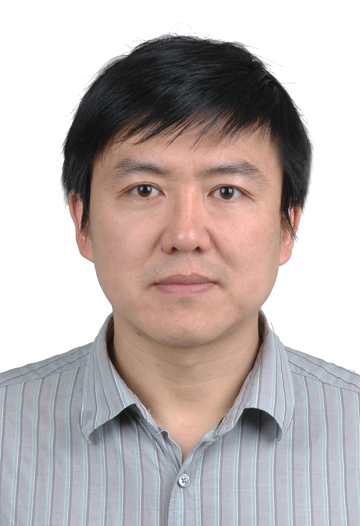 Chuan-Feng Li (李传锋)合作论文数University of Science and Technology of China;Key Laboratory of Quantum Information, Chinese Academy of Sciences18
 Guangcan Guo (郭光灿)合作论文数School of Physical Sciences, University of Science and Technology of China;Key Lab of Quantum Information, Chinese Academy of Sciences, University of Science and Technology of China18
 Jianshun Tang (唐建顺)合作论文数School of Physical Sciences, University of Science and Technology of China18
 Wei Liu (刘伟)合作论文数School of Chemistry & Chemical Engineering, Shaanxi Normal University16
 Zhipeng Li (李志鹏)合作论文数Department of Physics, Capital Normal University14Yuan-Ze Yang合作论文数CAS, Univ Sci & Technol China12Nai-Jie Guo合作论文数11Yi-Tao Wang合作论文数Key Lab Quantum Informat, Univ Sci & Technol China9
 Jin-Shi Xu (许金时)合作论文数School of Physical Sciences, University of Science and Technology of China9Lin-Ke Xie合作论文数8Yu Meng合作论文数7
 Shang Yu合作论文数7
 Shuang Wang (王双)合作论文数Chinese Academy of Sciences;University of Science and Technology of China4
 Qiang Li (李强)合作论文数School of Chemistry and Biological Engineering, University of Science and Technology Beijing4Xi-Wang Luo合作论文数Univ Texas Dallas, Dept Phys, Richardson, TX 75080 USA3
 Yang Mu (穆杨)合作论文数School of Environment, University of Science and Technology of China3
 Zongquan Zhou (周宗权)合作论文数School of Physical Sciences, University of Science and Technology of China3Pei-Yun Li合作论文数Univ Sci & Technol China, CAS Key Lab Quantum Informat, Hefei 230026, Peoples R China2
 Chengjie Zhang (张成杰)合作论文数School of Physical Science and Technology, Ningbo University2Si-Jing Tao合作论文数1Zhipeng Zhong合作论文数1Liang Chai合作论文数1
 Zhenghao Liu (刘正皓)合作论文数Information Retrieval Lab, Department of Computer Science and Engineering, School of Computer Science and Engineering, Northeastern University1Ji-Yang Zhou合作论文数1Tian-Xiang Zhu合作论文数1Wen-Hao Zhang合作论文数Univ Sci & Technol China, CAS Key Lab Quantum Informat, Hefei 230026, Anhui, Peoples R China1Zhe Chen合作论文数1Yu Du (杜宇)合作论文数1
 Shuo Deng (邓硕)合作论文数School of Physics and Mechanics, Wuhan University of Technology1Qinchuan He合作论文数1
 Yiqun Wang (王益群)合作论文数College of Materials and Chemistry & Chemical Engineering, Chengdu University of Technology1
 You Yu (于游)合作论文数Northwest University1
 Zhengwei Zhou (周正威)合作论文数School of Physical Sciences, University of Science and Technology of China1
 GuangLei Wu (吴广磊)合作论文数Institute of Materials for Energy and Environment, Qingdao University;College of Materials Science and Engineering, Qingdao University1Rongchun Ge合作论文数1
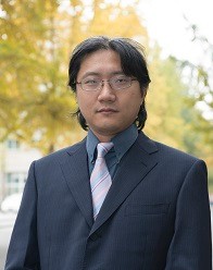 Xiao Liu (刘晓)合作论文数School of Physics, University of Electronic Science and Technology of China1
 Chuanyu Zhang (张传瑜)合作论文数Chengdu University of Technology1
 Song Li (李松)合作论文数School of Energy and Power Engineering, Huazhong University of Science and Technology1
 Raj B.Patel合作论文数Department of Physics, Faculty of Natural Sciences, Imperial College London1Liang Xu合作论文数1
 Yongjian Han (韩永建)合作论文数School of Physical Sciences, University of Science and Technology of China;Chinese Academy of Sciences1
 Ádám Gali合作论文数Wigner Research Centre for Physics, Institute for Solid State Physics and Optics, Hungarian Academy of Sciences1
 Shiyi Zhou (周世一)合作论文数College of Materials and Chemistry & Chemical Engineering, Chengdu University of Technology1




