This study proposes a quiescent current ($I\_{q}$) of 6.8 $\mu$A, maximum load current of 200 mA and external capacitorless low-dropout regulator (LDO) with an all-MOS reference. All MOS transistors, except for the power transistor $M\_{P}$ and the proposed current limitation transistor PM5, work in the subthreshold region, achieve ultra low $I\_{q}$. A complementary error amplifier with the NMOS and PMOS input pairs is adopted, as well as a push-pull stage with the miller compensation technique, to produce the main loop, where the dominant pole $p\_{1}$ and a second pole $p\_{2}$ are generated. The power transistor is implemented with an NMOS transistor, and it results in a high frequency pole $p\_{out}$ at the output node, even when the load capacitor ranges from 0 to 100 pF and the load current ranges from 100 $\mu$A to 200 mA. Meanwhile, Miller compensation causes a left half-plane zero $z\_{1}$ that compensates for $p\_{2}$, and the stability of LDO is well ensured. Due to the proposed LDO structure, a load-independent unity-gain-bandwidth (UGB) with a similar phase margin (PM) is achieved in this study. In addition, thanks to the adopted complementary error amplifier with a push-pull stage, the adopted fast feedback and the auxiliary feedforward paths consuming quite small external size and power, the power transistor is driven rapidly and a good transient response is achieved. The LDO proposed with reference is successfully implemented with a standard 180 nm CMOS process, and the active silicon area is approximately 0.12 mm$^{2}$. The measurement results show that the reference and output voltages are around 2.0 V. It achieves the measured maximum load current of 200 mA, and the total $I\_{q}$ is as low as 6.8 $\mu$A. It also achieves recovery time of less than 2.8 $\mu$s under different conditions (load current $I\_{L}$ steps from 100 $\mu$A to 200 mA and $C\_{L}$=0) with the load jump edge time $T\_{edge}$ of 2 $\mu$s. In addition, it achieves the maximum current efficiency of 99.996$\%$.
A 0.52% nonlinearity, 44.9 zF/root Hz input capacitance noise capacitance-to-voltage (C/V) converter for MEMS accelerometer is proposed in this study. The multi-step successive approximation (SA) output mechanism is proposed to replace the conventional single-step conversion. Meanwhile, combining with the modulation-demodulation (MD) technique in the traditional continuous-time (CT) C/V converter, a much lower nonlinearity and noise CT C/V converter without increasing power consumption is achieved in this work. In addition, a short time reset signal between modulation and demodulation is proposed to reset the integration capacitors in each conversion cycle, which lets the C/V converter achieve an approximate twice dynamic range enhancement (DRE). The proposed C/V converter is implemented in a standard 180 nm CMOS process. It incorporates an on-chip capacitor signal generator (CSG), whose capacitance is tuned from -80 fF to 80 fF using clock signals at frequencies of 10Hz, 1 kHz, 2 kHz, 3 kHz, 4 kHz, and 5 kHz respectively, where measurement results demonstrate that the converter has correct output voltage across this frequency range, with a conversion error of less than 350ppm/root Hz . The proposed C/V converter is also tested together with an integrated a MEMS accelerometer element. It achieves a maximum nonlinearity as low as 0.52% within +/- 10 g acceleration and obtains equivalent input noise power spectral density (PSD) as low as 44.9 zF/root Hz when the frequency is beyond 50 Hz.
This paper presents two level shifters (LSs) that achieve both low transmission delay ( $Delay$ ) and low energy consumption per transition ( $E_{t}$ ) for high-accuracy sensor applications, where VDDH is typically higher than 3V, and VDDL is near the threshold voltage. The first proposed level shifter, LS-CPFB, utilizes an all-MOS charge pump (CP) and a feedback control technique. The CP technique enables switches implemented with high-threshold-voltage (HTV) transistors to turn on rapidly. Both internal and feedback signals are employed to control the inputs of the latch-up circuit in LS-CPFB, resulting in reduced $Delay$ while maintaining low $E_{t}$ . Based on LS-CPFB, a second design, LS-FB, is proposed, where switches implemented with medium-threshold-voltage (MTV) transistors replace the HTV and standard-threshold-voltage (STV) transistors. With appropriate feedback control, LS-FB eliminates the need for the CP, achieving a significantly lower $E_{t}$ . For a fair comparison, both proposed LSs and three conventional LSs were implemented in the same 180 nm CMOS process. Simulation results demonstrate that LS-CPFB with VDDL of 0.6 V and VDDH of 3 V achieves both competitive $Delay$ of 2.12 ns and $E_{t}$ of 1.65 pJ, under an input signal VIN frequency of 1 MHz and an edge time ( $t_{edge}$ ) of 1 ns. Under the same condition, LS-FB achieves a competitive $Delay$ of 3.13 ns and the lowest $E_{t}$ of 0.93 pJ. The proposed LSs were fabricated, and measurement results show $Delay$ , $E_{t}$ , and static power dissipation ( $P_{s}$ ) consistent with simulation results obtained at the typical (TT) process corner, where $t_{edge}$ was limited to 15 ns by the test equipment. With 12 samples under room temperature, for LS-CPFB with the same VDDL, VDDH, and VIN in simulation, the average measured $Delay$ , $E_{t}$ and $P_{s}$ are 9.16 ns, 1.54 pJ, and 254 nW, respectively. For LS-FB, the average measured $Delay$ , $E_{t}$ and $P_{s}$ are 10.5 ns, 1.05 pJ, and 16 nW, respectively.
This article presents the design of a novel electronic door lock equipped with an infrared (IR) proximity sensor, two magnetic switches, and an electromechanical energy harvester. The power consumption of the embedded electronics is minimized with the IR proximity sensor, which keeps the system in sleep mode until the sensor detects the presence of a user and activates the system for card reading. Through careful component selection and effective power management, the system achieves a low sleep-mode current consumption of just 9.1 mu A, enabling fully batteryless operation. The electromechanical energy harvester is a three-phase AC generator and a rectifier that harvests energy from both the downward and upward lever motion exerted by users, via a latching relay, and stores it on two supercapacitors. The magnetic switches monitor both lever and door positions, controlling the latching relay and returning the system to sleep mode when the operation has finished. The door lock electronics also incorporates a near-field communication (NFC) card reader and a low-power microcontroller (MCU). Finally, a dual-channel driver drives both the relay and the door locking mechanism. Measurements demonstrate that a single door opening generates enough energy to complete a full cycle of card reading, door unlocking, and locking, with surplus energy providing an autonomy of 1.75 h for the next cycle. If this time is exceeded, the system can be recharged by simply turning the lever. To the best of the authors' knowledge, this work is the first demonstration of a batteryless electronic door lock in the literature.
This work presents the design and post-layout simulation of a cryogenic SiGe BiCMOS low-noise amplifier (LNA) for superconducting transmon-qubit readout in quantum processors scaling beyond hundreds of qubits. The target specifications are first established and justified by surveying state-of-the-art of cryogenic LNAs and modeling the dispersive qubit readout process. The LNA is implemented with three cascaded stages in common-emitter configuration and employs tuned inductive matching and parallel peaking networks in each stage to optimize noise, gain flatness, and bandwidth while maintaining minimal DC power consumption. The amplifier draws only 1.15 mW from a 0.15 V supply and occupies 0.252 mm(2). Post-layout simulations confirm input/output S-parameter matching better than -10 dB, 41-44 dB gain with <3 dB ripple, <5 K noise temperature across 4-9 GHz, and a worst-case OP1 dB compression point of -19.96.6 dBm. A comparative analysis demonstrates that SiGe BiCMOS offers a favorable trade-off between InP HEMT's low noise and CMOS's integration potential for large-scale quantum processors.
This paper presents a methodology for adjusting the BSIM-BULK model (formerly BSIM6) to simulate the behavior of NMOS and PMOS transistors at cryogenic temperatures, down to 4.2 K. The study analyzes existing characterization data for 28 nm bulk CMOS processes, identifying the threshold voltage (VTH), subthreshold swing (SS), and low-field mobility (mu 0) as the transistor parameters most significantly impacted by cryogenic temperatures. Based on this analysis, it is shown that VTH is expected to increase by 100-150 mV from 300 K to 4.2 K, SS approximately 60 mV/decade from 300 K to 4.2 K, and mu 0 increases, approximately doubling from 300 K to 4.2 K. In addition, a practical strategy is proposed to modify specific parameters that capture these temperature dependencies on the BSIM-BULK model. The different methods to verify the cryogenic behavior are described and applied to 3 mu m/28 nm NMOS and PMOS transistors at simulation level for validation.
This study proposes a 650 nA quiescent current and all-MOS transistors voltage reference without using amplifiers. To reduce quiescent current, all transistors working in the subthreshold region is implemented with a standard 180 nm CMOS process. A MOS subdivision circuit without using amplifiers and consuming quite low power is proposed to shift the reference voltage VREF1 of 0.35 V to a higher voltage level VREF around 2 V; meanwhile a high-order temperature compensation paths are also proposed to obtain a lower temperature coefficient (TC) for VREF. Measurement results showed that a total current as low as 650 nA and reference voltages around 0.35 V and 2.0 V are obtained. Without external trimming circuit VREF1 and VREF achieve a mean TC (temperature coefficient) of 573.9 ppm/degrees C and 435.3 ppm/degrees C respectively, where the temperature ranged from-40 to 85 degrees C.
Millimeter-wave radiometers can benefit from state-of-the-art on-chip technologies to construct a fully integrated front-end at frequencies above 100 GHz. The first step is to integrate a fully capable antenna design with a complex low-low noise amplifier in the same technology. This paper presents the integration simulation of a passive antenna array in IHP's SiGe 130 nm BiCMOS SG13G2 process and a 3-stage low-noise amplifier using the same technology. The final seamlessly integrated design proves to be a viable first building block for a future complete radiometer frontend-on-a-chip for frequencies exceeding 100 GHz.
This paper presents a square-law detector with a performance suitable for radiometric applications that is designed with the SiGe 0.13 mu m BiCMOS SG13G2 technology offered by IHP. The implemented topology is based on an HBT transistor in common-emitter topology with a differential output. The proposed detector is centered around 178 GHz and presents a great balance between the post-layout responsivity, noise, and power consumption performance when compared to the rest of the works of the SoA, with a simulated maximum responsivity of 160 kV/W, a minimum NEP of 1.37 pW/root Hz, and a power consumption of 0.32 mW.
Radio Frequency Identification (RFID) tags face inherent limitations in power delivery and communication range. Ultrahigh Frequency (UHF) offers extensive reach but microwatt power transmission, while High Frequency (HF) boasts better power delivery but suffers from restricted range. EPC UHF air protocol is very suitable for semi-passive RFID used as a sensor node in Internet of things (IoT) applications thanks to its backscattering ability reducing power consumption and allowing to achieve a high transmission range. But the low power delivery inherent in UHF often requires another power source. EPC standards also provide a HF protocol which can be used for better power delivery. This paper will investigate the potential gains of a dual frequency implementation through both EPC HF and UHF protocols and includes an FPGA implementation to demonstrate performance.
This paper introduces two Verilog-A blocks implemented in the Cadence Analog Environment as testbenches for integrating qubits with the electronics necessary for qubit state manipulation and measurement in circuit-level simulations. These blocks specifically model the control and readout mechanisms of transmon qubits, a type of superconducting qubit, by using key transmon and circuit parameters as inputs. The first block models the XY qubit control mechanism, simulating qubit state manipulation by a microwave driving pulse with adjustable shape, amplitude, and duration. It outputs the qubit state probability and the pulse parameters needed for arbitrary qubit rotations. The second block models the dispersive shift readout mechanism, providing the transient response of the qubit to a reading pulse. This block can determine the qubit state based on the pulse’s amplitude and phase and accounts for noise from the amplification stages. Simulation results using realistic transmon parameters validate the functionality of these Verilog-A blocks.
This paper analyzes the performance of a Fabry-Perot cavity antenna fed by an on-chip spiral antenna and compares it with an on-chip antenna designed to be integrated in IHP's 130nmSiGe BiCMOS chip in a 2x2 array configuration. The results show the increase in directivity obtained by the combination of the Fabry-Perot cavity and a single spiral antenna versus the directivity obtained by forming a complex sequentially rotated 2x2 spiral array.
In this paper different alternatives for the design of a Fabry-Perot cavity antenna operating in the Sub-mmwave frequency range and fed by a SiGe spiral antenna are evaluated. In particular a single spiral and a sequentially fed array of spiral antennas are compared, showing, due to the losses in the Si substrate the superior performance of the single fed cavity. However, the use of a sequentially rotated array significantly improves the Axial Ratio (AR).
This paper presents a BiCMOS low-noise amplifier (LNA) operating at G-band (140 to220 GHz) that is robust against harsh operation conditions, namely large temperature variations and radiation exposure. A SiGe technology (IHP's 0.13-mu m SG13G2) has been used for the amplifier design, due to its suitability for millimeter wave (mmW) frequencies and its built-in tolerance to total ionizing dose (TID)radiation. To address the impact of temperature variations on HBTs, the negative temperature dependence of the gain is compensated with a positive temperature dependent collector current, generated by the proposed on-chip and compact (0.0035 mm(2)) biasing circuit. It has a negligible degradation on the LNA performance, which shows a measured performance comparable with the state of the art with a minimum noise figure (NF)of 9 dB and a gain of 18.1 dB at room temperature, centered around 195 GHz and with a 3-dB bandwidth of 25 GHz. The measured gain and noise figure variations over a-20 degrees C to 80 degrees C temperature range are +/- 1.1 dB and +/- 1.5 dB, respectively. Finally, an experiment to study the TID radiation response of mmWLNAs is carried out. Fabricated samples are exposed to 250 krad(Si), 1.5 Mrad(Si) and 2 Mrad(Si), exhibiting a variation smaller than 1 dB in both gain and noise figure.
This paper presents a compact differential low-noise amplifier (LNA) with frequency tuning capability implemented with IHP's 0.13- mu m SG13G2 SiGe technology. Area efficiency is achieved with a semi-differential architecture, using compact transformers and avoiding the need of a Marchand balun. The frequency tuning capability is achieved with novel reconfigurable transformers that move the effective position of their center tap through 3 switches. The proposed reconfigurable transformers impose no penalty on the LNA performance, which shows a measured performance comparable to the State Of the Art. It covers at least from 140 GHz to 200 GHz with 5 different frequency operating modes and with a gain higher than 13 dB and a NF of 9.5 dB. Finally, temperature compensation biasing circuits are included to provide gain robustness against temperature, achieving a gain variation of less than 1.5 dB across 20 to 80 degrees C.
Simultaneous wideband input matching and gain performance while maintaining low core area is one of the big challenges of mmW amplifier design. In this work, the stacked common base (stacked CB) configuration is proposed for the input stage of an amplifier to achieve a good compromise between gain, input matching and area. The stacked CB topology is compared with the cascode and simple CB configurations to prove its validity. Finally, two G-Band amplifiers are designed with different input stage topologies: cascode and stacked CB. Both show very small core areas (0.066 and 0.085 mm 2 respectively) while maintaining gains of 22.8 and 22.5 dB, NF of 9.4 and 9.9 dB and GBW product of 317 and 346 GHz respectively that are comparable to the SoA. The stacked CB version shows a wideband input bandwidth of 76 GHz $(S11 < -10$ dB), making it a suitable choice for area-efficient and broadband input stages.
This paper presents a comprehensive overview and analysis of the state-of-the-art (SoA) in semi-passive or Battery-Assisted (BAP) Ultra-High Frequency (UHF) Radio Frequency Identification (RFID) sensor tags compliant with EPC Global G2/ISO-18000C. These tags operate on the same communication principle as fully passive sensor tags but incorporate a battery or an energy harvesting module. This additional power source extends communication ranges and enables power demanding applications using low-power microcontrollers (MCUs) and higher-end sensors. This article also analyzes various key features, including tag integrated circuit (IC) architecture, types of energy harvesting modules, and communication range. The main conclusions are threefold. Firstly, selecting the appropriate tag IC requires a careful analysis of its features such as sensitivity, sensor interfaces, or data logging capabilities. For instance, among the solutions examined in the SoA, half of them opted for a tag IC capable of MCU communication via SPI or I2C buses. Secondly, it is essential to assess both the forward and backward communication links to leverage the sensitivity of the tag IC in BAP mode. Interestingly, only one-third of the SoA solutions achieved the theoretical communication range anticipated by the sensitivity of the tag IC. Finally, an energy budget analysis is required to ensure that the energy generation suffices to meet the energy requirements of the tag. While most solutions rely on batteries as the energy source and analyze battery lifespan, only a few studies employing energy harvesters conduct an energy budget analysis due to the additional complexity involved.
A temperature compensated G-Band low-noise amplifier (LNA) is fabricated in IHP’s 0.13-µm SiGe BiCMOS technology. A biasing circuit is proposed, which compensates the complementary to absolute temperature (CTAT) dependence of the gain through a proportional to temperature (PTAT) collector current that is generated with an on-chip and compact (0.0035 mm 2 ) biasing circuit. Temperature stability is addressed without a penalty in the LNA, which shows a comparable measured performance from -20 °C to 80 °C to the State Of the Art measurements that are only offered at room temperature. The LNA is centered at 195 GHz with a 3 dB bandwidth of 25 GHz. The maximum nominal gain is 18.1 dB at room temperature and only shows a gain variation of ±1.1 dB from -20 °C to 80 °C. The minimum NF is 9 dB and has ±1.5 dB of variation in the temperature range.
This article presents a wireless temperature sensor tag able to work in both fully passive mode and in semi-passive mode when assisted by a flexible thermoelectric generator (TEG). The sensor tag consists of an EPC C1G2/ISO 18000-6C ultrahigh-frequency (UHF) radio frequency identification (RFID) integrated circuit (IC) connected to a low-power microcontroller unit (MCU) that samples and collects the temperature from a digital temperature sensor. With a temperature gradient as low as 2.5 °C, the test results show that the TEG provides an output power of 400 $\mu$ W with an output voltage of 40mV. Bymeans of an up-converter in order to boost the TEG output voltage, this harvester supplies the power required to the sensor tag for a 2-conv/s data rate in semi-passive mode. Moreover, when the tag operates in semi-passive mode, a communication range of 22.2 m is measured for a 2-W effective radiated power (ERP) reader. To the best of our knowledge, the proposed TEG-assisted sensor tag shows the longest communication range and the only one that provides stable external power at low-temperature gradients. The measured performance and the chosen architecture allow using the wireless sensor in multiple industrial or biomedical applications.
In this work we present a SiGe D-Band Low Noise Amplifier (LNA) for radiometric applications near the water absorption line at 183 GHz. The LNA covers the frequency range near 188 GHz with a peak gain of 23 dB and a minimum noise figure of 10.5 dB. Space hardening techniques are also presented in order to mitigate the LNA performance variation due to orbital changes and therefore, to achieve a more stable and constant sensitivity, NETD, of the radiometer. First, a current sensor is designed for bias changes monitoring caused by radiation. The reference voltages of the bias circuits are left as tuning-knobs to compensate the effect of radiation. Furthermore, this bias circuit also compensates the temperature dependence of the LNA. The gain variation is reduced from 11 dB to 2 dB and the NETD is keeped below 0.4. Thanks to these techniques a complete self-healing system could be implemented if they were extended with a processing block.
 H. Solar合作论文数42
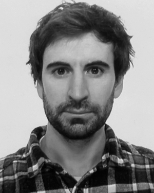 Del Rio, D.合作论文数Dept. of Electr., Nat. Univ. of Colombia;c;Dept. of Electr., Nat. Univ. of Colombia39
 Andoni Beriain合作论文数Communication IC Design Group (COMMIC), University of Navarra33
 Ainhoa Rezola合作论文数25
 Juan F. Sevillano合作论文数24
 Igone Velez合作论文数CEIT and TECNUN, University of Navarra19
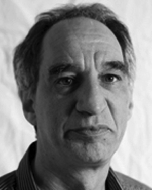 Iñaki Gurutzeaga合作论文数16
 Unai Alvarado合作论文数9
 Yang Xu合作论文数9
 G. Bistué合作论文数8
 Alvaro Urain合作论文数8A. García-Alonso合作论文数8
 Gui Liu (刘桂)合作论文数College of Electrical and Electronic Engineering, Wenzhou University8
 Juan A Montiel-Nelson合作论文数7
 Jaizki Mendizabal合作论文数7Hector Solar Ruiz合作论文数6
 Erik Hernandez合作论文数6
 Inigo Gutierrez合作论文数6
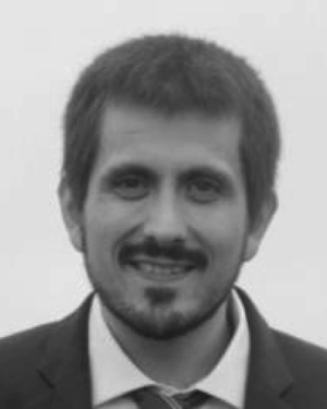 Zalbide, I.合作论文数6I. Rebollo合作论文数6Juan Meléndez合作论文数5
 Inigo Adin合作论文数5A. Jimenez-Irastorza合作论文数5Jose-Luis Gonzalez Jimenez合作论文数4J. Sosa合作论文数4e fernandez合作论文数4
 Ainara Jimenez合作论文数4
 Quanzhen Duan (段权珍)合作论文数School of Integrated Circuits, Sun Yat-Sen University4
 Mau-Chung Frank Chang合作论文数Hong Kong Institute for Advanced Study, City University of Hong Kong;University of California Los Angeles4
 Jon Legarda合作论文数Centro de Estudios e Investigaciones Técnicas de Gipuzkoa (CEIT) P° de Manuel Lardizabal4s garciaalonso合作论文数3i cendoya合作论文数3Abe Akhiyat合作论文数3Keya Kamtikar合作论文数3
 j de no合作论文数3
 Galarraga Inaki合作论文数3inigo ederraurzainqui合作论文数3Alberto Lopez-Gasso合作论文数3
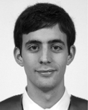 inaki fernandez合作论文数3Zhen Meng (孟真)合作论文数3Pardo, Daniel合作论文数3
 Vicente Gonzalez-Posadas合作论文数3
 Daniel Valderas合作论文数3
 Daniel Segovia-Vargas合作论文数Dept . of Signal Theory and Communications;University of Madrid;Dept . of Signal Theory and Communications, University of Madrid3R. Morales-Ramos合作论文数2I. Sancho合作论文数2J. M. Monzon合作论文数2Juan M. Herrera-Martín合作论文数2ibon zalbide agirrezabalaga合作论文数2




