Reliable integration of photonic integrated circuits (PICs) into quantum sensors has the potential to drastically reduce sensor size, ease manufacturing scalability, and improve performance in applications where the sensor is subject to high accelerations, vibrations, and temperature changes. In a traditional quantum sensor assembly, free-space optics are subject to pointing inaccuracies and temperature-dependent misalignment. Moreover, the use of epoxy or sealants for affixing either free-space optics or PICs within a sensor vacuum envelope leads to sensor vacuum degradation and is difficult to scale. In this paper, we describe the hermetic integration of a PIC with a vacuum envelope via anodic bonding. We demonstrate utility of this assembly with two proof-of-concept atom-interrogation experiments: (i) spectroscopy of a cold-atom sample using a grating-emitted probe; (ii) spectroscopy of alkali atoms using an evanescent field from an exposed ridge waveguide. This work shows a key process step on a path to quantum sensor manufacturing scalability. (c) 2025 Optica Publishing Group under the terms of the Optica Open Access Publishing Agreement
We present a method of optical magnetometry with parts-per-billion resolution that is able to detect biomagnetic signals generated from the human brain and heart in Earth's ambient environment. Our magnetically silent sensors measure the total magnetic field by detecting the free-precession frequency of highly spin-polarized alkali metal vapor. A first-order gradiometer is formed from two magnetometers that are separated by a 3 cm baseline. Our gradiometer operates from a laptop consuming 5 W over a USB port, enabled by state-of-the-art micro-fabricated alkali vapor cells, advanced thermal insulation, custom electronics, and laser packages within the sensor head. The gradiometer obtains a sensitivity of 16 fT/cm/Hz$^{1/2}$ outdoors, which we use to detect neuronal electrical currents and magnetic cardiography signals. Recording of neuronal magnetic fields is one of a few available methods for non-invasive functional brain imaging that usually requires extensive magnetic shielding and other infractructure. This work demonstrates the possibility of a dense array of portable biomagnetic sensors that are deployable in a variety of natural environments.
We present a set of building blocks for constructing and utilizing compact, microchip-based, ultrahigh vacuum (UHV) chambers for the practical deployment of cold- and ultracold-atom systems. We present two examples of chip-compatible approaches for miniaturizing UHV chambers—double-magneto-optical-trap cells and channel cells—as well as compact, free-space optical systems into which these cells can be easily inserted and quickly swapped. We discuss progress in atom chip technology, including miniature through-chip electrical feedthroughs and optical windows for transferring light between the trapping region on the chip and the ambient environment. As an example of the latter, we present some of the first through-chip fluorescence images of a Bose–Einstein condensate. High numerical apertures can be achieved with this technique, allowing for submicron resolution. Whether for optical detection, trapping, or control, such fine resolution will have numerous applications in quantum information, especially for experiments based on ultracold atoms trapped in optical lattices.
We present a technique for manipulating the dispersive properties of low index periodic structures using microfluidic materials that fill the lattice with various fluids of different refractive indices. In order to quantify the modulation of the optical properties of the periodic structure we use Equi-frequency contours (EFC) data to calculate the frequency dependant refractive index and the refractive angle. We further introduce various types of defects by selectively filling specific lattice sites and measuring the relative change in the index of refraction. Finally we design and optically characterize an adaptive low index photonic crystal based lens with tunable optical properties using various microfluidics. We also present experimental results for a silicon based PhC lens used an optical coupling element.
BACKGROUND:The analysis of single cells obtained from needle aspirates of tumors is constrained by the need for processing. To this end, we investigated two microfluidic approaches to measure the expression of surface proteins in single cancer cells or in small populations (<50 cells).METHODS:One approach involved indirect fluorescence labeling of cell-surface proteins and channeling of cells in a microfluidic device past a fluorescence detector for signal quantification and analysis. A second approach channeled cells in a microfluidic device over detection zones coated with ligands to surface proteins and measured rates of passage and of retardation based on transient interactions between surface proteins and ligands.RESULTS:The fluorescence device detected expression of integrin alpha5 induced by basic fibroblast growth factor (FGF-2) treatment in MCF-7 cells and that of Her-2/neu in SK-BR-3 cells compared with controls. Experiments measuring passage retardation showed significant differences in passage rates between FGF-2-treated and untreated MCF-7 cells over reaction regions coated with fibronectin and antibody to integrin alpha5beta1 compared with control regions. Blocking peptides reversed the retardation, demonstrating specificity.CONCLUSIONS:Immunofluorescence detection in a microfluidic channel demonstrates the potential for assaying surface protein expression in a few individual cells and will permit the development of future iterations not requiring cell handling. The flow retardation device represents the first application of this technology for assessing cell-surface protein expression in cancer cells and may provide a way for analyzing expression profiles of single cells without preanalytical manipulation.
We present a technique for manipulating the dispersive properties of low index periodic structures using microfluidic materials that fill the lattice with various fluids of different refractive indices. In order to quantify the modulation of the optical properties of the periodic structure we use Equi-frequency contours (EFC) data to calculate the frequency dependant refractive index and the refractive angle. We further introduce various types of defects by selectively filling specific lattice sites and measuring the relative change in the index of refraction. Finally we design and optically characterize an adaptive low index photonic crystal based lens with tunable optical properties using various microfluidics. We also present experimental results for a silicon based PhC lens used an optical coupling element.
We describe chip-scale batch-fabricated cesium cells utilizing semiconductor wafer processing, pin transfer of cesium, and silicon/Pyrex anodic bonding for cell sealing. High- speed, single-mode linearly polarized VCSELs emitting at the 133 Cs D1 line were fabricated, optimized for low threshold and high-speed operation with overall small power dissipation. Coherent population trapping (CPT) end-resonance signals with a contrast and linewidth of 5.4% and 7.1 kHz respectively are achieved using 1 mm optical path length cells and VCSEL driven with 1.25 mW RF modulation and 2.76 mW DC power dissipation. We demonstrate short-term stability of 4.5x10⁻¹⁰·τ-1/2 with an atomic clock built with these components operating on the CPT end-resonance. The magnetic field is stabilized with a novel magnetic field locking scheme tapping the Zeeman resonance.
 peter john zanzucchi合作论文数21satyam choudary cherukuri合作论文数19
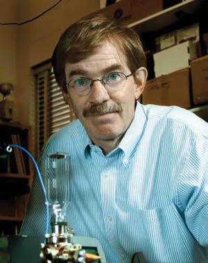 Dana Z. Anderson合作论文数Department of Physics, College of Arts and Sciences, University of Colorado Boulder;Infleqtion8pamela k york合作论文数6robert richard demers合作论文数6Joey Michalchuk合作论文数6aaron w levine合作论文数5
 Z. Hugh Fan合作论文数Microfluidics and BioMEMS Laboratory, Department of Mechanical and Aerospace Engineering, University of Florida5steven a lipp合作论文数4Rm Moroney合作论文数4
 James R. Matey合作论文数Department of Electrical and Computer Engineering, United States Naval Academy4Evan A. Salim合作论文数Department of Physics, University of Colorado4judith ann ladd合作论文数3robert leon quinn合作论文数3alan braun合作论文数3steven alan lipp合作论文数3william chiang合作论文数3charlotte a burton合作论文数3barry jay thaler合作论文数3m squires合作论文数3Joseph H. Abeles合作论文数sarnoff corporation3
 Richard P. Wildes合作论文数Department of Electrical Engineering and Computer Science, Lassonde School of Engineering, York University;Centre for Vision Research, York University3Peter Zanzucchi合作论文数3Jane C. Asmuth合作论文数3stephen charles hsu合作论文数2john g aceti合作论文数2William Holmgren合作论文数2christopher poux合作论文数2
 Dennis Prather合作论文数Department of Electrical and Computer Engineering, College of Engineering, University of Delaware2Robert D Whaley合作论文数2Gilbert L. Green合作论文数2
 Shouyuan Shi合作论文数2Raymond J. Kolczynski合作论文数2
 Kai M. Hudek合作论文数University of Colorado, and JILA, University of Colorado and National Institute for Standards and Technology2Matthew B. Squires合作论文数2Amrit K. Judd合作论文数2
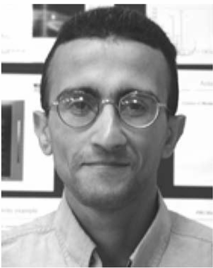 Sahar Ahmed-Sharkawy合作论文数Department of Electrical and Computer Engineering;University of Delaware;Department of Electrical and Computer Engineering, University of Delaware2david norman ludington合作论文数1paul heaney合作论文数1frederick j fritz合作论文数1john m margicin合作论文数1
 Stephen Hsu合作论文数1H An合作论文数1daniel m farkas合作论文数1Sh Dewitt合作论文数1CHERUKURI SATYAM C合作论文数1brad dinardo合作论文数1thomas squeglia合作论文数1a ulmer合作论文数1




